Continue to Site

Welcome to EDAboard.com

Welcome to our site! EDAboard.com is an international Electronics Discussion Forum focused on EDA software, circuits, schematics, books, theory, papers, asic, pld, 8051, DSP, Network, RF, Analog Design, PCB, Service Manuals... and a whole lot more! To participate you need to register. Registration is free. Click here to register now.

Charge pump don't increase the input voltage when output load is being placed

Status
Not open for further replies.

allennlowaton

Full Member level 5
Joined
Oct 5, 2009
Messages
247
Helped
3
Reputation
6
Reaction score
3
Trophy points
1,298
Location
Taiwan
Activity points
3,081
hello EDA fellows,

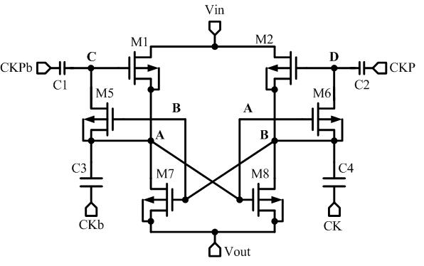
My designed charge pump performs well during no load condition.
But when I put the load, the output voltage don't increase sometimes it's lower as compared with the input voltage.
What happened? What should I do?

Thanks...
 

The load current is limited by capacitance of the flying capacitors and the operating frequency.
 
here is the circuit I used..
I got this from a paper.
How should I reinforce my charge pump?


---------- Post added at 13:24 ---------- Previous post was at 13:21 ----------

that pump should have an output of 80mA..The value of C1 and C2 I used were 1p and for the C3 and C4 were 100p.
I also tried to increased C3 and C4 to 1u but still it's no good.....

---------- Post added at 13:58 ---------- Previous post was at 13:24 ----------

my operating frequency is 1MHz...
 

... that pump should have an output of 80mA..The value of C1 and C2 I used were 1p and for the C3 and C4 were 100p.
I also tried to increased C3 and C4 to 1u but still it's no good.....my operating frequency is 1MHz...

Probably your MOSFET's (and, then, C1 & C2) and, possibly, your clock drive power are too small.
__
PS: Where's your GND reference node?
 
You need to add output capacitor (big enough to suppress voltage ripple) at Vout node.
 
Probably your MOSFET's (and, then, C1 & C2) and, possibly, your clock drive power are too small.
__
PS: Where's your GND reference node?

The ground reference node is located in between of the Cout and Rout at the output node.
 

80mA/1MHz = 80nC per cycle.
You have to compute if your charge pump can transfer greater than this charge every cycle.

You can also determine the maximum your charge pump can support by sweeping your load.
If you need to increase the load, you generally need either larger capacitances and/or higher frequency.
Also, you have to take into account other losses such as parasitic capacitances and cross-conduction currents.

thank you checkmate..
How to check / compute? The load current is a fixed value 80mA.
 

Status
Not open for further replies.

Part and Inventory Search

Welcome to EDABoard.com

Sponsor

Back
Top