Continue to Site

Welcome to EDAboard.com

Welcome to our site! EDAboard.com is an international Electronics Discussion Forum focused on EDA software, circuits, schematics, books, theory, papers, asic, pld, 8051, DSP, Network, RF, Analog Design, PCB, Service Manuals... and a whole lot more! To participate you need to register. Registration is free. Click here to register now.

Characterize a Mosfet Switch

Status
Not open for further replies.

AMSA84

Advanced Member level 2
Joined
Aug 24, 2010
Messages
577
Helped
8
Reputation
16
Reaction score
8
Trophy points
1,298
Location
Iberian Peninsula
Visit site
Activity points
6,178
Hi guys,

I'd like to know if someone can give me a tip on how I can characterize a MOSFET switch.

I'd like to make some plots but I really don't know which one's I should focus, that is, for example:

I though in plotting Vds VS Ids, Ids VS Vgs and think the Ron against what, Ids, Vgs? I though that those would be a good starting point but I don't know if I am thinking well.

The most important parameter here is the Ron but I would like to know how the MOSFET would behave with different values of Vgs and or Ids. Regarding the Vds, this Vds is the voltage across the transistor when in ON position. How can I predict the voltage here to make the simulation and with that get the Ron?

I am using Cadence & Spectre.

Regards.
 

Hi AMSA84

Read the attach file you will have some idea
 

Attachments

  • Effects-Of-On-Resistance-RON-To-An-Analog-Switch.pdf
    133 KB · Views: 190

Thanks for the reply. However this is not what I am looking for. What I would like to know is what are the relevant plot I should do (for instance, it is obvious that I must do first the Ids vs Vds, Ids vs Vgs).

I would like to do a good characterization of the transistor that I will be using in the technology that I will work. I'd like to do gds (R_on) vs Vds (?)(is the recommended one, to see how the ON resistance will vary with the Vds), I't like to do some plots where I can show the MOSFET capacitance (can anyone tell me how can I do this?) and any other that you guys can suggest me?

Regards
 

Relevant characteristics are Rdson versus Vgs, and Rdson versus temperature.
Usually, power transistors are used in the linear regime, i.e. at low Vds (so that Ids is proportional to Vds).
But in some applications, power devices operate at large Vds (and low Vgs) - in which case, characterizing Rdson dependence on Vds also makes sense.

Also important is Ids vs Vgs at various temperatures - it will show a "temperature compensated point" = a value of Vgs below which Ids increases with temperature increase (due to lowering Vt), and above which Ids is decreasing with temperature (due to a decrease in carrier mobility). Operation at Vgs below a temperature compensated point may be unstable with respect to temperature.

All the things mentioned above are related to DC operating conditions.

For transient operation, gate charge curves, capacitances - Cgs, Cgd, Cds - and their voltage dependencies, switching times, reverse recovery times, etc. are important.

You can look at any datasheet of a discrete power transistor, to see what characteristics are important.

Also, do not forget about various parasitics, always present in real designs/layouts, such as resistances of metallization, wirebonding, etc.
 

I suggest you begin with the application, know its "care-
abouts" and enumerate these. Then, the FET attribute
most relevant to each. Next, the FET terminal conditions
under which, you'd care about the care-abouts - with
particular emphasis on the worst cases (min/max gate
drive, min/max Vds, Vgs, Vgd, temperature, leakage
test conditions). Then you have the beginnings of an
orderly test plan.

A power switch, an RF switch, an analog switch and a
digital pass-gate all have somewhat different priorities
and datasheet parameters. Even though they're all ,
fundamentally, poly over glass over slab-o'-silicon.
 

In my case I need to characterize a Analago MOS Switch for a DC-DC Converter application (buck).

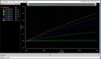
One thing that is making me confused is: Supposing that I am characterizing the SW at the DC op point. I know that the SW operates in the linear and in the cut-off regions. Now, to charact the SW we can grad a NMOS and put the source to ground and two power supplis to the gate and to the drain. Now, doing a parametric analysis sweeping the vds for different values of vgs we get the normal curves for the mosfet. However, I have to trace the same curves but taking into account that the MOS is to operate as a SW? In this case I do a sweep only to 100mV or so? Instead of 1.2V? (UMC 130nm) For different values of Vgs? I don't know which value is the VDSon, so how can I select a range of values for the Vds sweep?

I did that and I got this:


I am doing well? The thing here that is confusing me is how do I charact the SW taking into account the VDSon whithout knowing which value I'll get when the MOS is operating in the circuit.

Another thing. I want to plot the transistor RDSon and I was thinking using the S-Parameter. I have used that in the design of LNAs, VCO, MIXER, etc and I don't know if I can do the same here to get the RDSon. Can you help me out with that or there is another way? I tried, but I got stucked because I have to put there the operating frequency which doesn't make any sense for this purpose. A detail, I want to plot the RDSon VS W of the transistor. It's a good idea?
 

Status
Not open for further replies.

Part and Inventory Search

Welcome to EDABoard.com

Sponsor

Back
Top