Continue to Site

Welcome to EDAboard.com

Welcome to our site! EDAboard.com is an international Electronics Discussion Forum focused on EDA software, circuits, schematics, books, theory, papers, asic, pld, 8051, DSP, Network, RF, Analog Design, PCB, Service Manuals... and a whole lot more! To participate you need to register. Registration is free. Click here to register now.

Cadence Virtuoso Adder Layout help needed

Status
Not open for further replies.

Hassan Munir

Newbie level 6
Joined
Jan 27, 2012
Messages
14
Helped
0
Reputation
0
Reaction score
0
Trophy points
1,281
Activity points
1,409
Hi,

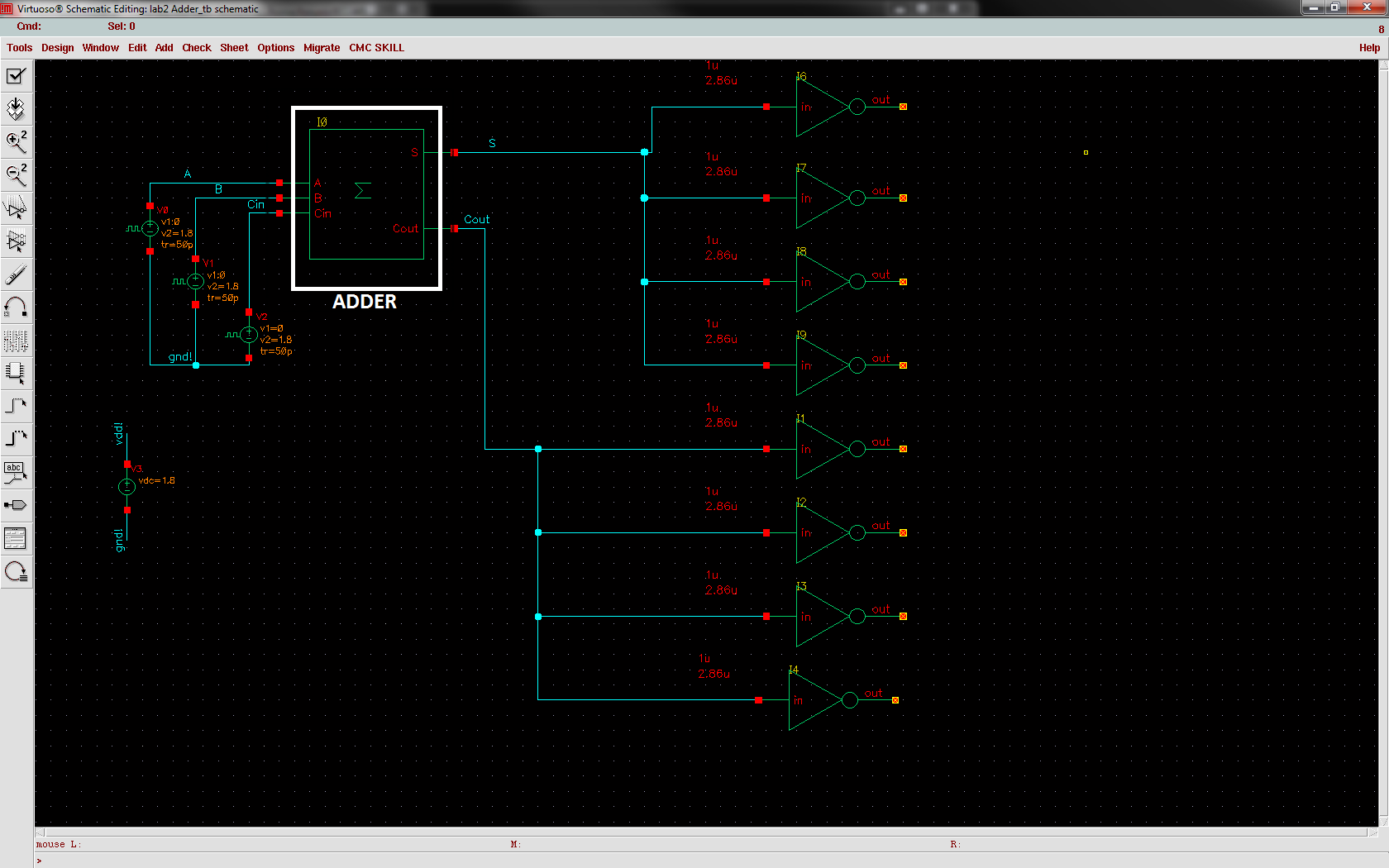
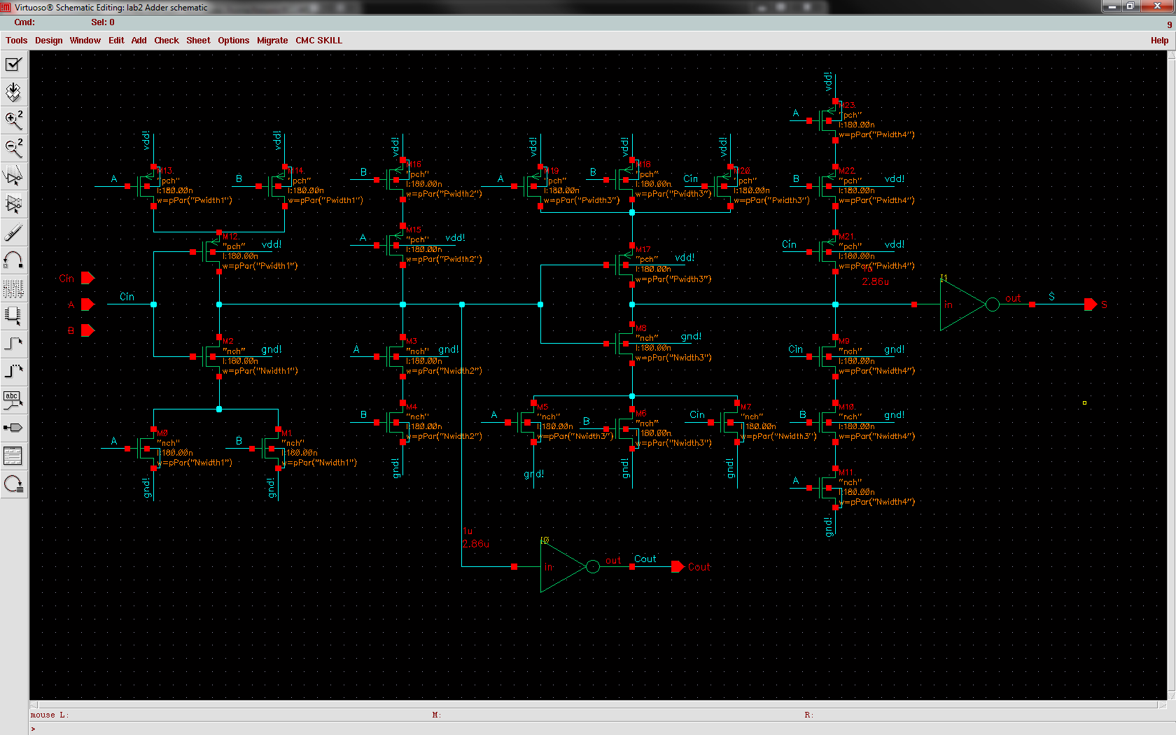
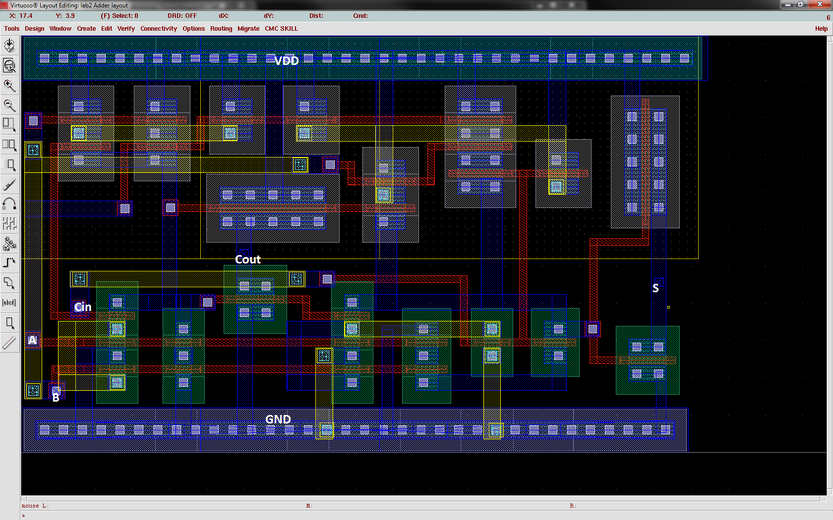
I created an adder layout as part of a university project using cadence virtuoso. Both DRC and LVS pass 100%. However when I simulate using my extracted view against my schematic view I see a huge discrepancy in terms of the output voltage swings( should be from 0 to 1.8V however extracted view gave me 0 to 500mV). I am using inverters at the output of both the sum and carry bits of the adder. The role of the inverters is to provide drive strength to the output to allow full voltage swing , so 500mV makes no sense. If LVS and DRC pass can there be reasons other than parasitic capacitance that can cause this issue. The lab required me to use metal 1 and metal 2 for routing. I followed manhattan routing so metal1 and metal2 are hardly ever parallel. So where could these parasitic effects come from?

Any help will be highly appreciated
 

Did you use current sources? If you only used one reference and routed it through the whole circuit there might be a voltage drop over your conductors, this will lower the current produced by each source (this is if you used a very large area).

Did you design your own gates or is this the gates of the foundry?
 

Thanks for the reply

No actually I did not use current sources and I did not create my own transistors. I generated the transistor from the schematic, rearranged them to optimize the area and routed them. Not sure if I performed bad routing as this is the first time I worked on layouts. This project is actually due in about 24 hours so please help

I have attached my layout, testbench and schematic for a clearer picture

https://obrazki.elektroda.pl/97_1341774569.png
https://obrazki.elektroda.pl/32_1341774569.png
https://obrazki.elektroda.pl/82_1341774569.png


At quick glance:

Did you remember that the width of your p-channel device should be n=Kn/Kp larger? doesn't seem like it from the layout. Look at the foundry buffers for reference. From the Layout it looks like n≈2.5.
 

I will look into that however how come the non layout based schematic simulation with p-channel width as above works perfectly with full voltage(0 to 1.8V) swing on S and Cout. So does the width rule for p-channel devices(n=Kn/Kp larger) apply to layout only and not the schematic?

Thanks
 

I am not entirely sure on how the simulator works and why this do not show, this is the first thing I saw which was wrong with the design. I know that the ratio mentioned above will influence your threshold voltage, it is more of a analog design rule but it shows in the digital side. I cannot guarantee that this is the solution, it is a start.

The equivalent ratios for nMOS and pMOS networks should be the same.

I did the digital design course a while back. The following is a good book for future reference on digital CMOS design:
CMOS Digital Integrated Circuits Analysis & Design by Sung-Mo Kang & Yusuf Leblebici from McGraw-Hill with ISBN:978-0072460537

 
Last edited:

Thanks for the help,

I got it working. My mistake was that the global nets vdd! and gnd! were not defined properly in the layout and hence the supply rails in the layout were not being powered.
 

Status
Not open for further replies.

Part and Inventory Search

Welcome to EDABoard.com

Sponsor

Back
Top