sorata
Junior Member level 1
HI,all
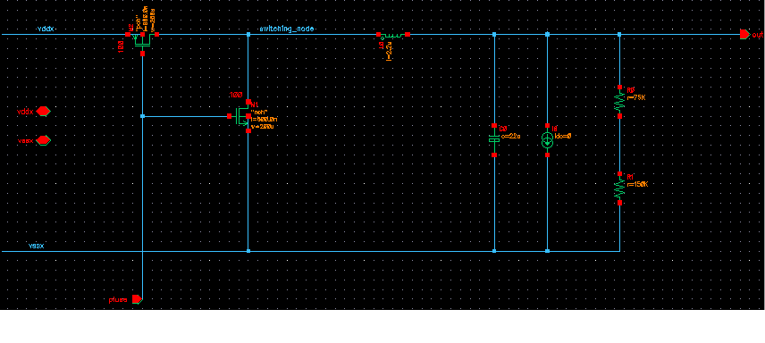
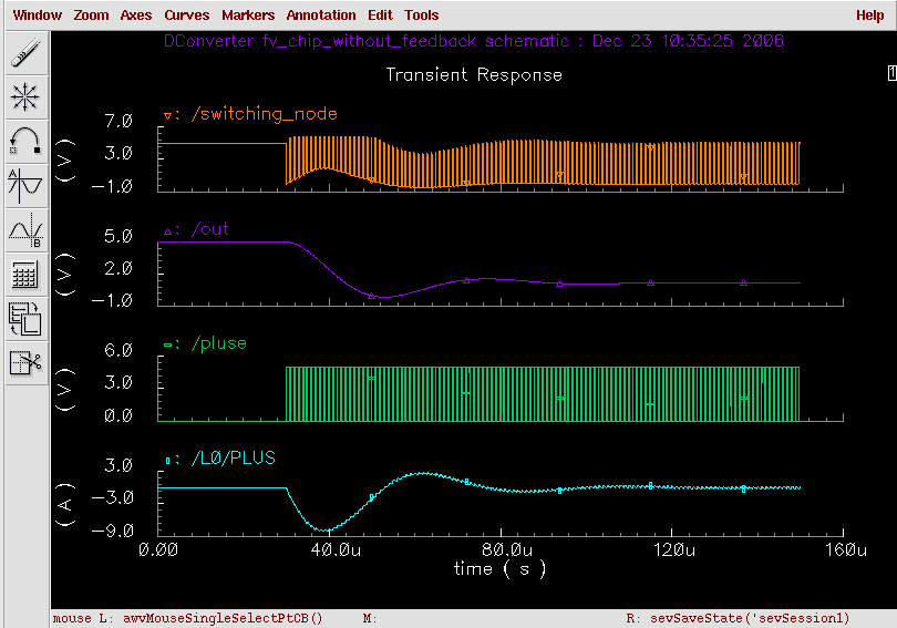
I am implementing a buck dc/dc converter, voltage-mode. The wave of Vout should act as Figure 1(by Matlab model) . but in my circuit implementation, the Vout starts with high voltage , then oscillates as Figure 2(by circuit implementation).
any instructions is welcome,thanks!
add conditions: the input is 5V dc voltage, i want to get 1.2V vout. I simulated the circuit with no load current. and the feedback voltage is scaled to 0.8V for the negative input of error amplifier. The ramp signal is showed in Fig 2(/ramp).
br,
Figure 1
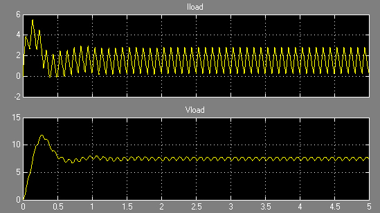
Figure 2
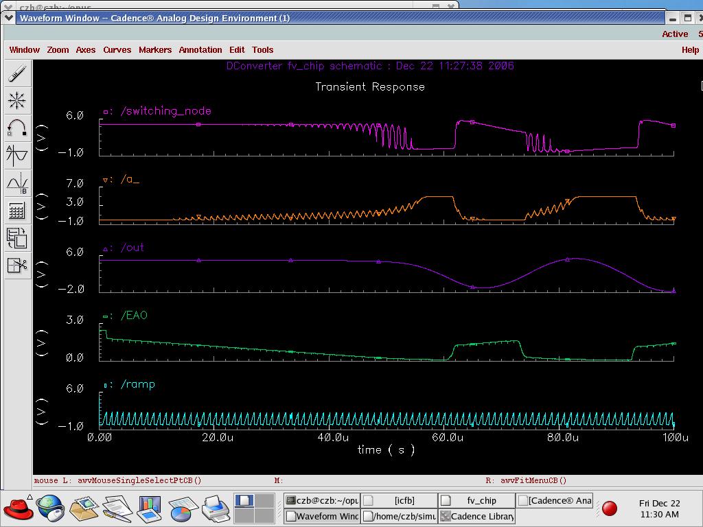
I am implementing a buck dc/dc converter, voltage-mode. The wave of Vout should act as Figure 1(by Matlab model) . but in my circuit implementation, the Vout starts with high voltage , then oscillates as Figure 2(by circuit implementation).
any instructions is welcome,thanks!
add conditions: the input is 5V dc voltage, i want to get 1.2V vout. I simulated the circuit with no load current. and the feedback voltage is scaled to 0.8V for the negative input of error amplifier. The ramp signal is showed in Fig 2(/ramp).
br,
Figure 1
Figure 2