mtwieg
Advanced Member level 6
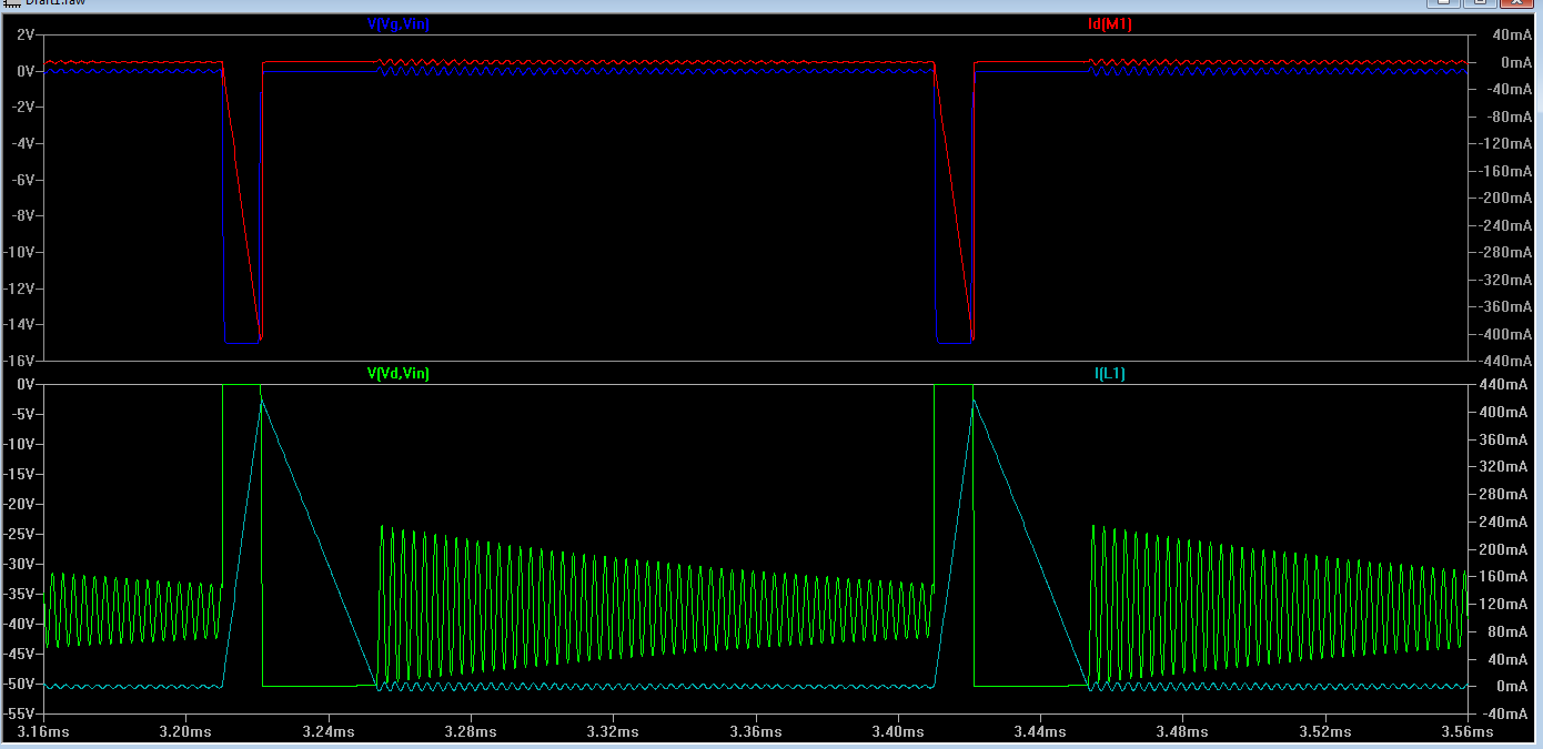
Yes, though with FETs it's the linear region, not saturation.Dear Friend , my mean is that the P mosfets are alike with N mosfets but with this difference that if the voltage across the GS of them become -15 volt the will be at saturation region .
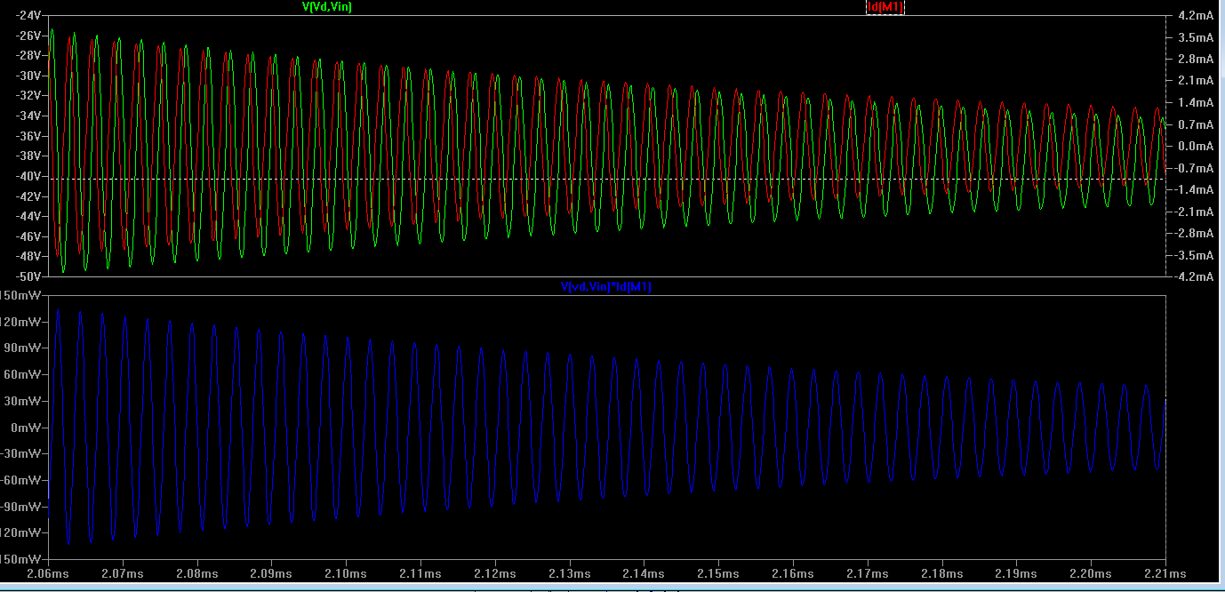
That equation for conduction losses is valid while the FET is conducting. You can see from the waveforms where Vgs is pulled negative and the FET is on (the red trace is gate voltage). But the ringing has nothing to do with those conduction losses. So I'm still waiting for you to explain why you believe the ringing affects dissipation/efficiency.so with this considerations , the efficiency equation and loss power equation will be equal with NMOSFET . isn't it ?
")