Continue to Site

Welcome to EDAboard.com

Welcome to our site! EDAboard.com is an international Electronics Discussion Forum focused on EDA software, circuits, schematics, books, theory, papers, asic, pld, 8051, DSP, Network, RF, Analog Design, PCB, Service Manuals... and a whole lot more! To participate you need to register. Registration is free. Click here to register now.

Bubba Oscillator and THD

Status
Not open for further replies.
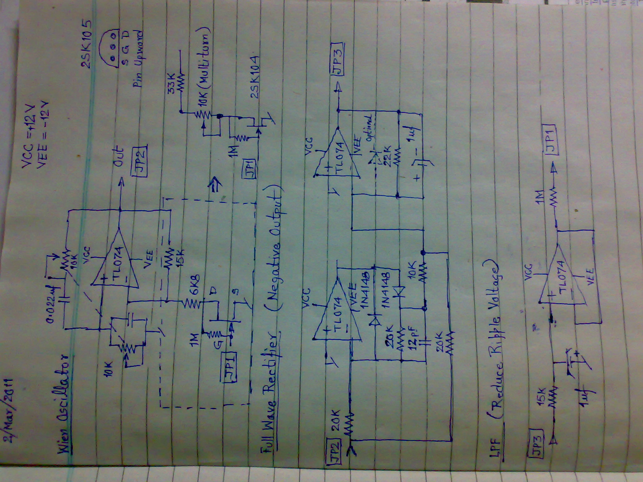
Actually I measured the resistance of lamp and I found the higher one was 4.7E so I thought using higher resistance (in hundred or kilo range) would make the net effect of lamp resistance negligible.

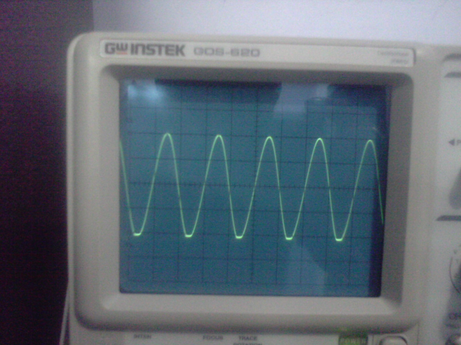
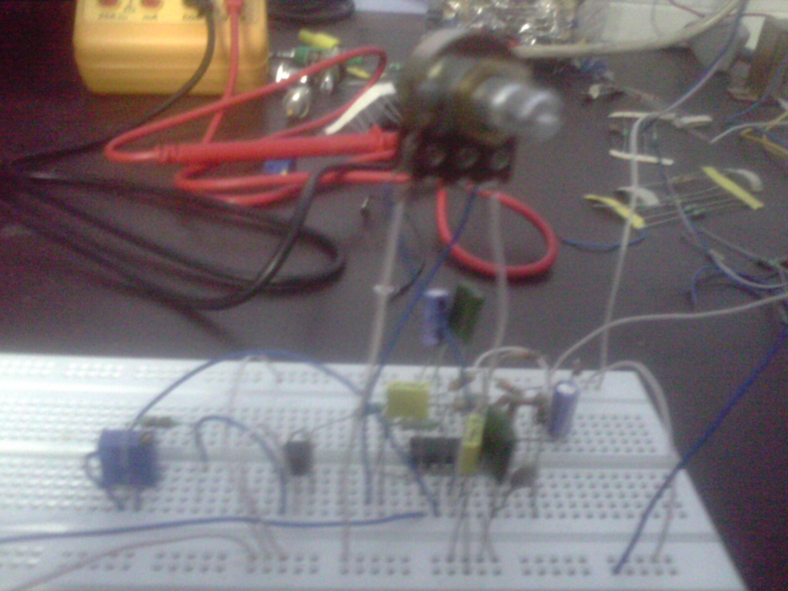
My first attempt gave me much confidence. On 2/Mar/2011 I'll breadboard Wien with FET AGC.

---------- Post added at 13:23 ---------- Previous post was at 13:17 ----------

One more question can I use LPF to lower the ripple effects in AGC loop ?
 

I didn't mean, that a different resistor dimensioning would help with the lamp PTC design. If the filament resistance is too low, you can't operate the circuit with usual operational amplifier. And you won't want to add a power amplifier, because it increases THD.

One more question can I use LPF to lower the ripple effects in AGC loop ?
You have to pay attention to the control loop's phase margin. If the low-pass corner is considerably above the loop unity gain frequency, it's possible.
 
Sameer, I repeat: I do not recommend a PTC (lamp) for stabilization purposes. The temperature characteristic is to sharp/steep.
A thermistor with an NTC-characteristic is much better suited for this task. And you have many many more options to select the needed combination between nominal resistance and thermal behaviour (B value).
 
If the low-pass corner is considerably above the loop unity gain frequency, it's possible.

As per rule of thumb (not precise) how much difference should be there between ripple frequency and LPF corner frequency ?

A thermistor with an NTC-characteristic is much better suited for this task.

I'll try to find out suitable NTC.
 

The temperature characteristic is to sharp/steep.
At low filament temperatures, it isn't. But as you most likely don't find incandescent lamps with a filament resistance compatible to OP circuits, I agree about the practical suggestion.

---------- Post added at 10:38 ---------- Previous post was at 10:05 ----------

how much difference should be there between ripple frequency and LPF corner frequency ?
The critical point is the loop phase margin, it's not directly related to oscillator respectively ripple frequency. I suggest to try the effect of loop gain, filter time constant and possibly additional low-pass filters on ripple and loop transient response in a simulation.
 

Hi LvW and FvM,

Yesterday I breadboard the entire circuit but FET did not work. Circuit is working fine up to LFP (before FET).

Could you please tell me the method to determine Gate, Drain and Source pins with DMM (I am confused with 2SK104 and 105) and how to measure RD(on) because I am unable to find their data sheet.

I have also ordered J-111 (Fairchild Vgs min -3V max -10V) which will be delivered to me in next 15-20 days.
 

Gate can be identified with a multimeter by the diode junction. Rdson can also be measured with a multimeter, it's basically around Vp/Idss.
 

FvM could you please elaborate the steps involved. Small setup will greatly enhance the visualization.

How to identify Drain and Source ?
 

Drain and source can't be distinguished electrically, and for a symmetrical JFET they can be exchanged without any effect.
 

LvW : Actually i am intrested in making an audio band oscillator with lowest possible distortion. I am touching electronics field after more than 12 years of inactivity so please forgive my mistakes.

When we needed a very-low distortion sine wave source (less than 0.01%), we used an audio card in a computer and programmed it as needed using MIDI commands. We used the digital output (S/PDIF) as an input to the device under test, but you could use a decoder IC (such as the NXP UDA1355H) to generate an analog signal.

Burr-Brown (owned by Texas Instruments) makes some of the lowest THD opamps available. You should check out their catalog.

Jeff
 

Last night I managed it to work but there are issues

1. Clipping occurs at negative swing and the swing is 20V pk-to-pk (which is very high).
2. Oscillation does not start until I vary potentiometer in Gain setting arm (connected in series with FET). I have to vary potentiometer each time.

I measured it's Vp (2SK104 = 1.26V), 2SK105 died during testing.

Is the Rdson resistance which we use to dimension the feedback network ?


Sameer, the pictures you have presented are not very informative; more important: What is the actual circuit? (Bubba, Wien or something else?)
In particular, how does the negative feedback path looks like? Ootherwise, nobody can comment/evaluate your results.
 

What is the actual circuit? (Bubba, Wien or something else?)
Post #81: On 2/Mar/2011 I'll breadboard Wien with FET AGC.

Sameer, the pictures you have presented are not very informative
I apologise. Here is the circuit.


Sameer, thank you.
Regarding the complete rectifier circuitry it is not easy to decide (without simulation) if it works properly.
But I have one recommendation: Check (measure/simulate)
(a) the gate control voltage vs. time,
(b) the drain voltage vs. time.
 

LvW: If you have time could you please simulate the circuit at your end.

I'll measure them tonight.

I'm new to FETs. One thing I noticed while identifying gate pin is that gate (+ probe) to Pin-X ( - probe) DMM's diode test function showed 732 and to Pin-Y ( - probe) 1453. Then using resistance mode I connected probes to Pin-X and Pin-Y resistance was 4.26K. Is it normal behaviour ?
 

The FET measurements sound strange to me. A usual JFET should show an equal diode voltage drop (650-750 mV) for the forward biased gate-drain and gate-source junctions, and infinite resistance for the reversed bias. The measured drain-source resistance would be near to Rdson, if you don't allow a considereable voltage drop (by using a higher resistance range). The value depends on the FET type and ranges from a few 10 ohm (with low resistance switch/high gm RF FETs) up to several kohm.
 
A usual JFET should show an equal diode voltage drop (650-750 mV) for the forward biased gate-drain and gate-source junctions.
This is the point which alarmed and forced me to post the measured results.

Does it mean that I must replace the FET ?

if you don't allow a considereable voltage drop (by using a higher resistance range).
Range setting was 20K and also measured with 200K.
 

Sameer, at the moment, I can give you some general recommendations only because
(a) I have your fet not in my library and (b) because I leave for two days.
Recommendation:
*When the output amplitude is to large (clipping) the regulation mechanism must be activated at smaller amplitudes. That means, the N-JFET must operate (steady state) at a smaller voltage (magnitude) - equivalent to a smaller RDS,on. Therefore, the feedback resistor (15 k) must be reduced to keep the ratio of both resistive branches. Try this.
On the other hand, take care, that the signal voltage drop across the DS-path is not to large (not more than 50...100 mV max). From this requirement you can calculate the series resistor (presently Rs=6.8k) and a suitable feedback resistor.
*Example: With Rf=15k and Rs=6.8k the nominal RDS,on=15k/2-6.8k=0.7k.
With RDS,on=700 ohms and Rf=15k the voltage across DS is app. 4% of the output voltage.
That means for Vout=12 V (maximum) the voltage across DS is app 0.5 volts. perhaps a bit to large for a good THD.
* Check the FET characteristik in conjunction with the control voltage that is available after rectification
* Check the rectifier circuit separately with a sinusiodal input from a generator.

Good luck
 
Sameer,
I couldn`t find the datasheet for the selected FET, but I have tried to make some general considerations, which I think apply more or less to this FET type:
Ids,s=10 mA
Vp=-2 V.

The result is enclosed (Rds vs. V,gate). The applied drain voltage is Vds=0.5 volts.
It can be seen that the FET control voltage (at the gate) should be around (-1.6...-1.7)V and the corresponding resistance is app. (0.5...1) kohms.
The other areas are not well suited for control purposes (slope of the curve to large or to small, respectively).
Perhaps, this information can support your investigations.
 

Status
Not open for further replies.

Similar threads

Part and Inventory Search

Welcome to EDABoard.com

Sponsor

Back
Top