Continue to Site

Welcome to EDAboard.com

Welcome to our site! EDAboard.com is an international Electronics Discussion Forum focused on EDA software, circuits, schematics, books, theory, papers, asic, pld, 8051, DSP, Network, RF, Analog Design, PCB, Service Manuals... and a whole lot more! To participate you need to register. Registration is free. Click here to register now.

Boost PFCs in parallel? (Average current mode)

Status
Not open for further replies.

cupoftea

Advanced Member level 5
Joined
Jun 13, 2021
Messages
2,664
Helped
54
Reputation
108
Reaction score
116
Trophy points
63
Activity points
14,007
Hi,
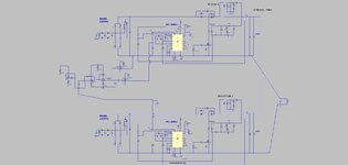
Here is an improvement on the 2 paralleled Average current mode Boost PFCs.

The attached (LTspice and jpeg) is 2 paralleled Boost PFCs. Each is grounded to a slightly different potential, as is often the case in adjacent high current SMPSs.
Anyway, in order to be paralleled, one is Master, and the other is Slave. The Slave has its Current Error Amplifier input as being the same as that of the Master. Obviously each PFC sits on a slightly different ground, so a Diff Amp is needed to pass the Masters Current Error Amplifier input voltage to the Slave.

The attached shows it being done. Can you think of a lower component count way of doing this?

(As you may note, the simulation has been made “quicker-to-run” by forcing a fixed voltage into the Voltage Error Amplifier’s input. In the actual simulation, each PFC would have a feedback divider from the Vout, as normal.)
 

Attachments

  • PFCs in pllel_diffamp.jpg
    PFCs in pllel_diffamp.jpg
    105 KB · Views: 152
  • LT1248 Boost PFC paralleled_diffamp.zip
    6.3 KB · Views: 120

Hi,
Having such loops laid out in your schematic - how would you avoid them on the pcb ?

My personal opinion:
* there is no need for the schematic to be physically organized like the PCB. Not even in parts.
In first place the schematic should as clearly as possible show the connections and the function of the circuit.
Genrally I recommend to use symbols for GND and power supply and so on ... they have no physical meaning for the PCB.
Indeed I don´t like the - non standard - schematic symbols that more show the package of a device than it´s function. In my eyes it makes not much sense to have a schematic symbol with the pins ordered 1-2-3-4... like the package.
Especially with OPAMPS and logic devices where you just see the (package) pin numbers.. where you need to have the datasheet by hand to find out which pin number is the non-inverting input and which is the power supply.

But..
For sure - if it does not hurt readability - it makes sense to show special wiring informations: like where the kelvin connection is placed.

At schematics I prefer the signal (information) flow from left to right (which has nothing to do with PCB) and the higher supply voltage on top the sheet and the most negative supplies at the bottom of the sheet.
On a schematic I may have 4 OPAMPs spread - mabe on multiple schematic pages.. where on the PCB they all are in one package.

***
In the above schematics I don´t like the lengthy POWER and GND nets. I´d rather use symbols or labels.
I don´t like the non 0°/90° lines especially those useless bends, and the unnecessary crossings.
And most of all: they are too small (in resolution) so one can not find out the part values not the pin names.
I miss the power supply decoupling capacitors that are essential when designing power switching applications.

In most cases the schematics should help you. But as soon as the schematic is used for other persons (customer, repair, forum...) it helps if they are easy to read.

But I´ve seen way worse schematics.

Klaus
 

Thanks, this has been very valid.....AYK, it has turned into a "schematic topology format" post. -A very worthy cause....and particularly salient here, where we are paralelling SMPS's and so risk these dreaded layout afflictions.

(I know another schematic format....the higgledy-piggledy format......carried out by many UK based consultancies, so that the customer is impeded as much as possible from doing the design , or any further mods, themselves...but need to always pay the consultant to do it, since they cant get to grips with the schem in its higgledy... format)

However, might i now beg advice on the paralleling of two AvCM Boost PFCs by duplicating the Master's MOUT pin voltage to the slave's?...as in post #20.

Does the schem of post #20 depict the best way to "copy over" the MOUT pin of the Master to the slave?
Can you see any lower component count methods to do this?
 
Last edited:

" Hi, Here is an improvement on the 2 paralleled Average current mode Boost PFCs. ... "

There is a much better chance this power circuit will work as intended - but no guarantee ( layout dependent ) that the bridge rectifiers will share current - in fact the hotter one will tend to hog the majority ...
--- Updated ---

As to KlausST - if the schematic is not drawn in a way that imparts useful information as to power paths, kelvin connections and similar - it is unlikely that a pcb layout derived from same will be a 1st time winner.

A lot of very useful information can be imparted from a schematic with differing line widths and careful layout to show the viewer the importance of various regions and how to avoid noise pickup, radiating loops and other behaviour or mis-behaviour that may or may not be sought ....
 
but no guarantee ( layout dependent ) that the bridge rectifiers will share current
Thanks, for your advice on Bridge rectifiers in parallel. The schem in #20 uses just the one bridge rect. so we would assume this one is OK(?)
 

Status
Not open for further replies.

Similar threads

Part and Inventory Search

Welcome to EDABoard.com

Sponsor

Back
Top