Continue to Site

Welcome to EDAboard.com

Welcome to our site! EDAboard.com is an international Electronics Discussion Forum focused on EDA software, circuits, schematics, books, theory, papers, asic, pld, 8051, DSP, Network, RF, Analog Design, PCB, Service Manuals... and a whole lot more! To participate you need to register. Registration is free. Click here to register now.

Boost PFCs in parallel? (Average current mode)

Status
Not open for further replies.

cupoftea

Advanced Member level 5
Joined
Jun 13, 2021
Messages
2,802
Helped
55
Reputation
110
Reaction score
120
Trophy points
63
Activity points
14,785
Hi,
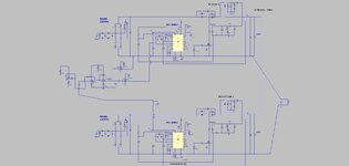
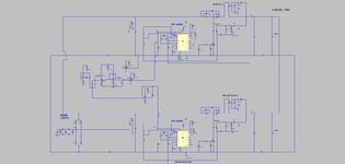
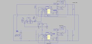
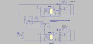
Here is an improvement on the 2 paralleled Average current mode Boost PFCs.

The attached (LTspice and jpeg) is 2 paralleled Boost PFCs. Each is grounded to a slightly different potential, as is often the case in adjacent high current SMPSs.
Anyway, in order to be paralleled, one is Master, and the other is Slave. The Slave has its Current Error Amplifier input as being the same as that of the Master. Obviously each PFC sits on a slightly different ground, so a Diff Amp is needed to pass the Masters Current Error Amplifier input voltage to the Slave.

The attached shows it being done. Can you think of a lower component count way of doing this?

(As you may note, the simulation has been made “quicker-to-run” by forcing a fixed voltage into the Voltage Error Amplifier’s input. In the actual simulation, each PFC would have a feedback divider from the Vout, as normal.)
 

Attachments

  • PFCs in pllel_diffamp.jpg
    PFCs in pllel_diffamp.jpg
    105 KB · Views: 185
  • LT1248 Boost PFC paralleled_diffamp.zip
    6.3 KB · Views: 134

This is great fallacy often conjured up by newbie engineers - trace all possible return paths for the current and you will see why ...
Thanks, woops, my apologies, i accidentally just copied and pasted them in....it should be like in the attached, ie, both boosters fed by the same diode bridge.
I added different ground resistors so each booster controller is grounded to a slightly different potential, but the potential of their MOUT pin to "local" ground, is the same, courtesy of the opamps.
Can you see opportunities for lowering the component count?
 

Attachments

  • LT1248 Boost PFC paralleled_diffamp_1.zip
    6 KB · Views: 116
  • LT1248 boosts in pllel.jpg
    LT1248 boosts in pllel.jpg
    149.5 KB · Views: 121

Can you think of a lower component count way of doing this?

As an answer...
This topology seems to want to jump into the spotlight. Ordinary bridge voltage doubler. 2 caps, 2 diodes.

I once built one to power a xenon timing light for our car. It should be satisfactory to go with an unchanging load. The coupled inductor serves to limit current to the system (as well as reduce spike-y behavior). Adjust Its value so as to obtain your desired voltage at the load.

Output voltage isn't easy to self-regulate. There's more than one method although all require greater complexity and greater work.

Voltage doubler 230VAC coupled inductor limits to 400VDC to load 4A.png
 

Thanks, ...
The solution of #4 is no different to what you get with a dual PFC using UCC28070A controller

There is admittedly some "simulation abbreviation" going on, but the essence is that they have the same "demand" input to the current error amplifier...so therefore they will both have the same current throughout.....one of them has a vout divider which helps set its current error amp reference. The "slave" is set up so that its MOUT pin output current gets gobbled up by the opamp......however, i think i know what you are referring to...the LT1243 may not like having an opamp into its MOUT pin......and maybe it needs more circuitry so that the MOUT pin is set up so that it outputs max current, then a diode pulls down on MOUT to ser its voltage......i will dig this out and post it.....its more components, but as i believe you possibly imply(?).....it avoids connecting an opamp output directly to the MOUT pin.

I am pretty sure ive posted such a solution before on this platform...so i will google seek with as follows...
site:edaboard.com/forums/power-electronics PFC


....Aah OK, here is the correction.....now there is no direct opamp input to the MOUT pin.....so this will work with the 2 PFCs in pllel (LTspice and jpeg as attached)
The slave is hacked so its MOUT pin outputs max current...the opamp is connected to it via a diode, and pulls down the MOUT pin (MOUT1) to the correct value....so no damage to the MOUT pin....and master and slave have the same MOUT pin voltage....so they share the current..

There is no vout feedback.....so yes, it woudlnt work....but one can imagine the attached with master having vout feedback......(the sim takes way too long to run if you put in vout feedback unfortunately)
 

Attachments

  • Pllel PFC _MOUT to MOUT.jpg
    Pllel PFC _MOUT to MOUT.jpg
    150.6 KB · Views: 121
  • LT1248 Boost PFC paralleled_diffamp_2.zip
    6.1 KB · Views: 98
Last edited:

Actually, the attached is the finished version for ACM Boost PFCs in parallel.
In this one, the "slave" is set up so that it spews maximum current out of its MOUT pin all the time......the opamp connected to slave MOUT pin then sucks in this current (via the diode shown), so that the MOUT pin of the slave , is at the same potential (relative to its local gnd), as the master's MOUT to its local ground.

...sorry that was a mouthfull to explain!

I believe now that finally, the mystery of the paralleled ACM Boost PFCs, has been solved.

No minor feat, when you consider that the bandwidth of a Booster PFC, is too low for the likes of "load share" chips such as UC3902 or UC3907.

As before, there is no vout divider because the sim takes hours and hours to run if a vout divider is used....so instead, a fixed voltage is put into SS pin.....one just has to pretend that a vout divider is used into the master.
 

Attachments

  • LT1248 Boost PFC paralleled_diffamp_3.zip
    6.1 KB · Views: 103
  • Pllel PFC _MOUT to MOUT 1.jpg
    Pllel PFC _MOUT to MOUT 1.jpg
    145.8 KB · Views: 98

that's pretty funny - still won't work in the real world - build it and you will see - as said before - this has caught out a lot of newbies ... topology is ( often ) everything ...

[ BTW your layout is considerably different to the TI one you posted ].
 
BTW your layout is considerably different to the TI one you posted
Thanks, i am not sure what you mean by "layout"?....as you know, i havent posted any PCB Layouts.

The attached is an improvement on the above....it has another opamp added to stop the MOUT pin of the slave ever going below its local ground.

still won't work in the real world
Thanks, i believe you are referring to the injection of a voltage into the SS pin(?)....i agree......but as explained above it must be done like this otherwise the sim takes till xmas.... please just pretend the master has an output divider in the normal way.

this has caught out a lot of newbies ... topology is ( often ) everything ...
AYK, the topology shown is in no doubt, they are 2 PFC Boost converters....paralleled
 

Attachments

  • LT1248 Boost PFC paralleled_diffamp_4.zip
    6.2 KB · Views: 96
  • Pllel PFC _MOUT to MOUT 2.jpg
    Pllel PFC _MOUT to MOUT 2.jpg
    152.2 KB · Views: 107
Last edited:

Respectfully - you have completely missed the point, which was plainly stated as topological, as to layout - one lays out a schematic too - all the info is there - you just need to read, rather than skim.
 
Thanks, AYK...this is just one Boost PFC...with another one alongside it....the "other one" (AKA slave) has the same voltage between its current error amplifier input and ground, as with the master.
Are you saying its not possible to "implant" this signal voltage at the said current error amplifier input ?

I am actually wondering if a better method (for paralleling Boost PFCs) would be to have the two LT1248's right next to each other, with a full ground plane beneath them...so that they both have the same ground, so to speak....then go from there..?

....then as such, we would get them "sharing" by setting the "slave" up with its voltage error amplifier as a follower...and just shovel the error amp voltage of the master, to the slave....only the master woudl have the vout divider.................done like this, we really are pretty much doing it like the gracious (but lonely) UCC28070A. (I say lonely, because UCC28070A is the only controller on the market for ACM Boost PFC's in parallel).

...however, as the following shows....UCC28070A may be a problem child.....

LT1248


...hence it is wanted to solve the "parallel ACM Boost PFC conundrum".
 
Last edited:

If the above "pllel ACM Boost PFC with duplicated current error amp input" doesnt work.....then i am sure you would agree that it could work if the controller was made discreetly, such that the current error amp input voltage was duplicated properly........i mean, the "idea" works. Just that offtheshelf ACM Boost PFC control chips are not conducive to the "method"?
 

Thanks, in post #3 you speak of tracing all the return paths....but there, you refer to the schem of the first post, with the two rect bridges, which was indeed a mistake by myself....the circuit then got re-drawn as per the UCC28070A, and with a single rect bridge.....

If we look at the page 13 of UCC28070A datasheet...we can see that the two current error amp inputs are joined together....that is essentially what i am trying to achieve with the two LT1248's......if it works with ucc28070A, then i would think it would work with two LT1248's.........not ignoring the fact that its more challenging to make these inputs the same in voltage when using two LT1248's.....thats what all the opamps are about in #10's schem.

UCC28070A
 
Last edited:

"the circuit then got re-drawn as per the UCC28070A, and with a single rect bridge....."

the re-drawn ckt has the same topological fault as the 1st ....
 
the re-drawn ckt has the same topological fault as the 1st ....
Thanks, ive just traced it out again (#10 above) with my eyes..the topolgy is boost and is correct for a boost. Whatever is the problem that you are speaking of.....it isnt recognised by the LTspice simulator.
The LTspice sim works fine. (#10 above)

I had expected contentions to be raised about the situation of implanting the voltage on the master's MOUT pin to the slave's MOUT pin. It seems odd that no objection has been raised about this....because surely, if theres anything contentious about the above (#10), then its the act of doing that?

BTW, im sure you appreciate, the resistors in the ground are simply rough stray trace resistance resistors...ie, not "resistors" really.

Im also quite literally staggered that over all the web and forums and App Notes, there's no real solutions given for putting ACM Boost PFCs in parallel....ie, using standard ACM Boost PFC chips.......there are solutions for doing it with a micro, yes.....and i even confess...when i reverse engineered a 3kW Dual Boost PFC battery charger, the two boost PFCs werent truly in parallel.......one was running for 10ms, then the other for 10ms, ....repeatedly.

So the situation of the Dual AvCM Boost PFC , is a mystery
 
Last edited:

the re-drawn ckt has the same topological fault as the 1st ....

Thanks, do you refer to the unfortunate large ground loop which is evident in the schem of #10 above?.......i can assure that this would not be there in the actual PCB layout.

Also, maybe you think the Paralleled AvCM Boost PFCs of #10 above wouldnt work because of the use of Current sense transformers, without having a Duty cycle limit circuit in there? (so that the current sense transformers could have adequate time to reset)........one such thing would actually be added, but unfortunately isnt included in the sim as it already takes ages to run.
 
Last edited:

" Thanks, do you refer to the unfortunate large ground loop which is evident in the schem of #10 above?.......i can assure that this would not be there in the actual PCB layout. "

Having such loops laid out in your schematic - how would you avoid them on the pcb ? can you draw a schematic ( representative of an actual pcb copper tracking arrangement ) that avoids them ?
 
Thanks, yes, the attached shows the Dual Boost PFCs schematically re-drawn so as to deter the implemtation of large GND loops on the PCB.
 

Attachments

  • LT1248 boosts in pllel.jpg
    LT1248 boosts in pllel.jpg
    151.5 KB · Views: 105
  • LT1248 Boost PFC paralleled_diffamp_7.zip
    6.2 KB · Views: 86

Status
Not open for further replies.

Similar threads

Part and Inventory Search

Welcome to EDABoard.com

Sponsor

Back
Top