Continue to Site

Welcome to EDAboard.com

Welcome to our site! EDAboard.com is an international Electronics Discussion Forum focused on EDA software, circuits, schematics, books, theory, papers, asic, pld, 8051, DSP, Network, RF, Analog Design, PCB, Service Manuals... and a whole lot more! To participate you need to register. Registration is free. Click here to register now.

Boost converter

Status
Not open for further replies.

odaysaad

Newbie
Newbie level 1
Joined
Dec 16, 2021
Messages
1
Helped
0
Reputation
0
Reaction score
0
Trophy points
1
Activity points
17
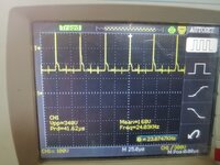
I have design interleaved boost converter with three inductor operates with 3pwm with phase difference 120 degree..iput voltage 12 volt and output voltage 168 volt but with high spike in output voltage can any one help me to reduce the spike in output voltage please
 

Attachments

  • IMG_20211209_111811.jpg
    IMG_20211209_111811.jpg
    4.5 MB · Views: 70

KlausST

Super Moderator
Staff member
Advanced Member level 7
Joined
Apr 17, 2014
Messages
23,263
Helped
4,741
Reputation
9,503
Reaction score
5,126
Trophy points
1,393
Activity points
154,109
Hi,

How can we help, what is your idea?

From the scope picture we can see the spike, but you don't give us any chance to see where it comes from.
We don't see at which signal you measure, we don't see your scope's GND connection.

* post your schematic
* post your PCB layout
* post photos
...

You are not the first one with spike problems. Thus there are already numerous discussions.
Read through some of them, then you get a clue what to look and care for.

Klaus
 

dick_freebird

Advanced Member level 7
Joined
Mar 4, 2008
Messages
8,230
Helped
2,292
Reputation
4,594
Reaction score
2,332
Trophy points
1,393
Location
USA
Activity points
65,835
First you need to determine whether the "spike"
is real, or a 'scope grounding / pickup-loop
artifact.

High-ESR, high-ESL filter cap at the output is a
good way to see leading edge "spikes" as the
cap is not acting as a cap against high dV/dt.
Show your output filter (if any). Show the load.

14:1 is a pretty high boost voltage ratio. You
might be better off with a flyback, so some or
most of the boost can come from turns ratio?
 

BradtheRad

Super Moderator
Staff member
Advanced Member level 7
Joined
Apr 1, 2011
Messages
14,750
Helped
2,871
Reputation
5,754
Reaction score
2,887
Trophy points
1,393
Location
Minneapolis, Minnesota, USA
Activity points
110,242
Notice the inductor has to generate a power pulse much higher than 168V. If it doesn't then it fails to overcome output voltage.

The pulses are narrow. They have to provide all power used during idle periods. It looks as though you're measuring voltage at the node joining inductor, switch, diode.
 

shomikc

Member level 4
Member level 4
Joined
Apr 19, 2013
Messages
71
Helped
0
Reputation
0
Reaction score
0
Trophy points
1,286
Activity points
1,951
Try having a look at the inductor and capacitor values and modify your calculations if necessary or if possible. I think lowering the inductor value might help. If the load is inductive you could try placing an appropriate free wheeling (anti-parallel) power diode or a schottky diode for high frequency. If you can simulate your circuit in Orcad PSpice I think you will get a better idea of what is going on.
 

dick_freebird

Advanced Member level 7
Joined
Mar 4, 2008
Messages
8,230
Helped
2,292
Reputation
4,594
Reaction score
2,332
Trophy points
1,393
Location
USA
Activity points
65,835
Here's another thought, it appears there's a lot
of ringing but decimated by the'scope timebase.
Maybe the switch device wants a properly tuned
snubber? You don't perhaps need the snappiest
turnoff, mellowing it out ought to reduce any
inductance related (cap ESL, wireball, load
characteristic) overshoots.
 

cupoftea

Advanced Member level 5
Joined
Jun 13, 2021
Messages
1,861
Helped
45
Reputation
90
Reaction score
88
Trophy points
48
Activity points
9,568
What is your power level?
I think you may need each boost to be a cascaded boost....two boosts controlled by one controller.

[B]dick_freebird[/B] was right 14:1 is high.

(i dont know why im stuck on bold now sorry)
--- Updated ---

How much c(out) do you have?
Can you see us the volts across yoru source sense?
 

asdf44

Advanced Member level 4
Joined
Feb 15, 2014
Messages
1,000
Helped
355
Reputation
710
Reaction score
344
Trophy points
1,363
Activity points
9,709
Yeah correlate those spikes to events in your circuit. Is it each fet switching or maybe only one phase?


As said figure out if it’s real: attach scope gnd to your circuit then attach the scope probe to its ground. That shows scope pickup.
 

Easy peasy

Advanced Member level 6
Joined
Aug 15, 2015
Messages
4,275
Helped
1,340
Reputation
2,680
Reaction score
1,727
Trophy points
1,393
Location
Melbourne
Activity points
23,891
the spikes are mostly artifact getting into your scope, there will be a little bit of overshoot - but not that much ....

for Brad - the boost inductor supplies Vout - Vin, volts, if it has to overcome significant L in the output loop then the boost-L will supply a lot more volts to keep the current flowing - so layout may well be an issue for this ckt - but we don't know as we can't see the layout ...
 

dick_freebird

Advanced Member level 7
Joined
Mar 4, 2008
Messages
8,230
Helped
2,292
Reputation
4,594
Reaction score
2,332
Trophy points
1,393
Location
USA
Activity points
65,835
Another possibility (as we still do not know anything about schematic, layout and applied control signals) is that the spike -is- the boost phase, petering out to the VIN-Vf forward push, and then the switch turns on again setting output current to zero; repeat....
 

Status
Not open for further replies.

Similar threads

Part and Inventory Search

Welcome to EDABoard.com

Sponsor

Top