Continue to Site

Welcome to EDAboard.com

Welcome to our site! EDAboard.com is an international Electronics Discussion Forum focused on EDA software, circuits, schematics, books, theory, papers, asic, pld, 8051, DSP, Network, RF, Analog Design, PCB, Service Manuals... and a whole lot more! To participate you need to register. Registration is free. Click here to register now.

[SOLVED] bjt cascode design problem

Status
Not open for further replies.

fareen

Full Member level 3
Joined
Oct 31, 2010
Messages
154
Helped
4
Reputation
8
Reaction score
4
Trophy points
1,298
Activity points
2,193
hello,
i'm designing a bjt cascode for my electronics lab i need sum help.
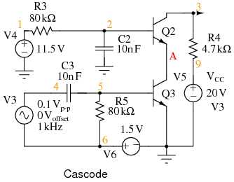
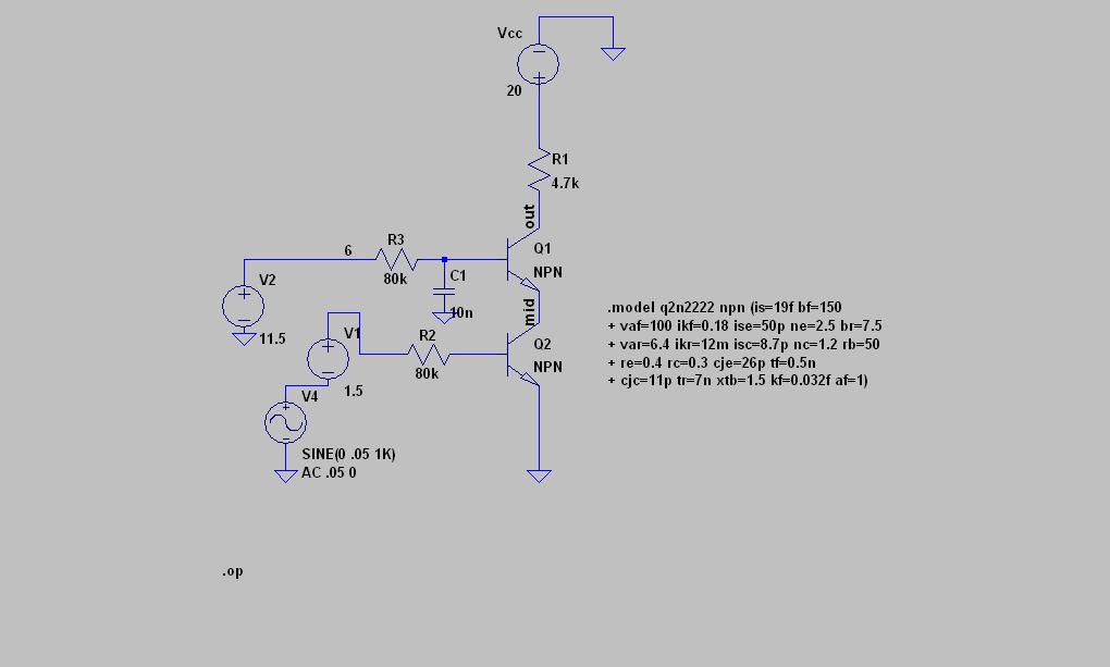
i took the circuit from the following link .i simulate it on lt spiece the gain obtained from graph is 4.2 but calculations show a much bigger gain like in thousands i can not understand the error??
The cascode amplifier : BIPOLAR JUNCTION TRANSISTORS


---------- Post added at 11:35 ---------- Previous post was at 11:07 ----------

the calculated gain is the factor of beta but the its quite low,why??/
 

The input voltage is divided down by R2 and then amplified. Why?
 

r2 is the base resistance that is required for the biasing of transistor so that it remain in the active region while the small signal input is not effected by r2(base resistance).we are mainly concern about the small signal gain ignoring the baising parameters
 

while the small signal input is not effected by r2
How did you come to this consideration? You may wan't to perform a detailed calculation of the small signal gain.

Or simply change the circuit to comply with the original one from the literature.
 

like how???
im missing sumthing can you explain more???
i am unable to attach the spice circuit here??
 

like how???
I'm referring to the differences between your above LTSPICE circuit (R2 is acting as signal attenuator) and the original cascode circuit

9_1303846303.jpg
 

connecting circuit like this as shown in figure gives the following transfer function\
--- Transfer Function ---

Transfer_function: -4.49385e-015 transfer
v4#Input_impedance: 1e+020 impedance
output_impedance_at_V(out): 4700 impedance
--- Transfer Function ---

Transfer_function: -7.92351e-016 transfer
v4#Input_impedance: 1e+020 impedance
output_impedance_at_V(mid): 820.494 impedance


this kind of transfer function is not correct so i connected it that way but still does not give the required output.
 

The numbers sound absurd:

Transfer_function: -4.49385e-015 transfer
v4#Input_impedance: 1e+020 impedance

I don't understand what you did exactly. Why not simply posting the LTSPICE *.asc design?
 

the problem is im unable to upload the lt spice file its giving error,unsupported file???
how can i do it??:(
 

Simply pack the *.asc file to zip or other supported archive format.
 

yeah thanks nice idea :)
 

Attachments

  • bjt cascode.zip
    818 bytes · Views: 44

The circuit is just fine. .tf is however a DC small signal transfer function that doesn't make much sense with AC coupling. Just use the same small signal analysis as in the original circuit
.ac dec 10 1k 100Meg
In addition, to directly display the gain, the V4 AC voltage should be set to default 1V. The level doesn't count in small signal, except for the gain calculation.
 

1v ac voltage clip the output waveform.
i need to verify the gain obtained from the graph with the calculation using formulas in the attachment.
the measured gain and the gain calculated is very different.
i dont know why?
 

Attachments

  • BJT Cascode.pdf
    27.2 KB · Views: 80
  • bjt cascode.zip
    818 bytes · Views: 40

1v ac voltage clip the output waveform
Apparently, you didn't yet understand the nature of small signal simulation. 1V is just a number in this regard, could be 1 kV without problems. The important point is gain normalization, for this reason, AC 1V has been selected in the original literature and I prefer the same.
the measured gain and the gain calculated is very different
I get 47.3 dB (231), which isn't very different from 261 from your calculation.
 

i know im very dumb with these analysis
plz could u explain how u calculate 231 gain from the 47.3 db??

---------- Post added at 16:40 ---------- Previous post was at 16:20 ----------

and also if we want to calculate the gain from tranisent analysis who would it be??
 

dB to voltage gain: 10^(47.3/20) = 231
You can also set the LTspice magnitude display axis to linear or log instead of dB.

To measure based in transient analysis, you have to determine e.g. vout Vpp.
 
  • Like
Reactions: fareen

    fareen

    Points: 2
    Helpful Answer Positive Rating
gain =vout/vin
vout vpp =3.84V
vin =0.1Vpp
gain=38v/v
is this correct???
[Apparently, you didn't yet understand the nature of small signal simulation. 1V is just a number in this regard, could be 1 kV without problems. The important point is gain normalization, for this reason, AC 1V has been selected in the original literature and I prefer the same.]
i didnt understand this logic.
 

gain =vout/vin
vout vpp =3.84V
vin =0.1Vpp
gain=38v/v
is this correct???
Calculated correctly. But it's not the true amplifier gain, because 1 kHz is far below the lower cut-off frequency of the AC coupling. You get maximum gain at about 100 kHz, where you need to reduce the input voltage to 0.01 Vp.

i didnt understand this logic
It's about the insignificance of voltage numbers in small signal analysis. They haven't to do with real voltage limits, they are just relative quantities to calculate gains.
 

Thanks a lot now i get it:)
 

Status
Not open for further replies.

Similar threads

Part and Inventory Search

Welcome to EDABoard.com

Sponsor

Back
Top