Continue to Site

Welcome to EDAboard.com

Welcome to our site! EDAboard.com is an international Electronics Discussion Forum focused on EDA software, circuits, schematics, books, theory, papers, asic, pld, 8051, DSP, Network, RF, Analog Design, PCB, Service Manuals... and a whole lot more! To participate you need to register. Registration is free. Click here to register now.

Bizarre thermal interface pad

Status
Not open for further replies.

mtwieg

Advanced Member level 6
Joined
Jan 20, 2011
Messages
3,908
Helped
1,311
Reputation
2,628
Reaction score
1,435
Trophy points
1,393
Visit site
Activity points
30,026
Recently for a contract I'm working on, I opted to use a themal pad for a thermal interface between some surface mount FETs and an aluminum heat spreader. I've had experience with silicon TIMs before, but for this I wanted to try something with better thermal performance so after looking for a while I found the PC94 material and bought some to use. Now that I've got it in my hands, it's a lot different from what I expected.

First, it has the feel of a gummi candy, or chewed bubble gum, only much thinner. As in it can be easily stretched and torn with little effort. It's very soft, but has a very "tacky" surface. In the product datasheet, it gives a curve of thermal impedance and compression vs pressure, which is the main piece of info I used to select it. But now that I can feel how soft this stuff is, that curve doesn't seem right, and lo and behold if I go on **broken link removed** I find **broken link removed** which is completely different (the datasheet linked on that page gives the first curve...). I've sent an inquiry about the discrepancy, no reply yet.

Anyways, my real question is how one should handle a soft, fragile thermal pad like this, including in a high volume manufacturing process? I imagine it would be pretty easy to cut with a simple punch. But for actually applying and assembling it, how would that be done? It's as limp as a wet noodle, so it takes me a bit of coaxing to get it to lie flat in the right position, I can't imaging how a machine could do it. Or are these kind of things always hand assembled anyways?
 

What do you think about to use heatsink tape ?

heat-sink-tape-250x250.jpeg


+++
 
  • Like
Reactions: mtwieg

    mtwieg

    Points: 2
    Helpful Answer Positive Rating
The different curves are for "deflection" only. Do you know how deflection of the materials is exactly defined? I don't. Does the 100% deflection point mean, the material is completely displaced at 40 psi?

I guess, the differences might be related to different test setups or sheet thickness, which can vary between 0.25 and 5 mm.

Generally, suitable structuring methods can't be discussed without knowing the application geometry and requirements. Major manufacturers of thermal isolation and gap filler materials (Bergquist, Laird) have a large portfolio of different products to choose from.
 
  • Like
Reactions: mtwieg

    mtwieg

    Points: 2
    Helpful Answer Positive Rating
What do you think about to use heatsink tape ?

heat-sink-tape-250x250.jpeg


+++
From what I understand, thermal tape is generally very thin. I am trying to bond several SMT components to a heatsink, and their surfaces won't be perfectly coplanar, so I need something with decent compliance. Also the heatsink will be mounted rigidly to the enclosure, meaning the gap between the heatsink and the PCB will vary a bit, and so a relatively thick, elastic interface is desired.

The different curves are for "deflection" only. Do you know how deflection of the materials is exactly defined? I don't. Does the 100% deflection point mean, the material is completely displaced at 40 psi?
I assumed this was the case, until I saw those curves that go up to 100% deflection. I can't imagine what else it could mean though. And no literature on the manufacturer's site is helping out.
Generally, suitable structuring methods can't be discussed without knowing the application geometry and requirements. Major manufacturers of thermal isolation and gap filler materials (Bergquist, Laird) have a large portfolio of different products to choose from.

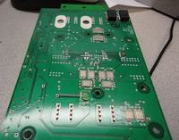
Okay, so here is the bottom of the PCB, all the flat metal packages are FETs.


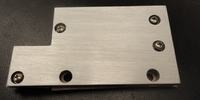
The PCB is housed in an aluminum box, and there's about 6mm of space between the PCB bottom and the floor of the box. I have machined aluminum pieces to fill most of this gap, as shown:


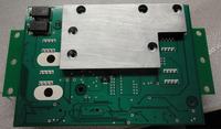
It should fit onto the PCB like this:


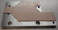
The face of the aluminum shown in these pictures will contact the flat enclosure floor, with some general thermal grease. But the other side of the heatsink is the tricky part, since it must conform to the lumpy electronics. So I use some TIM:


To give you an idea of how this stuff is, here's a picture of what happens when two pieces are pressed together and left alone for a while:


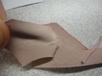
They literally fuse together. And they are very stretchy, up to when they tear in a raggedy fashion:


Like I said, it's just like chewed gum. I don't have a picture, but after assembling and then disassembling the thing, the FETs leave very deep imprints in the TIM, and they don't seem to relax back into a flat surface. So it seems like this material has a very low yield strength, and deforms plastically. I was hoping that it would be the opposite, and I could rely on the TIM providing some pressure on the FETs, but apparently it won't.
 

I already guessed that you are using this kind of chipscale-packaged power FETs. As a specific problem, it's difficult to get them soldered in an exactly flat position, so some kind of thermal gap filler or a special solder procedure seems necessary. There are possibly more elastic materials availabe, but in my view, a plastic gap filler is best fitting the requirements. The main drawback is that you can't unmount the heat spreader without removing the gap filler and applying new material.
 

Status
Not open for further replies.

Similar threads

Part and Inventory Search

Welcome to EDABoard.com

Sponsor

Back
Top