Continue to Site

Welcome to EDAboard.com

Welcome to our site! EDAboard.com is an international Electronics Discussion Forum focused on EDA software, circuits, schematics, books, theory, papers, asic, pld, 8051, DSP, Network, RF, Analog Design, PCB, Service Manuals... and a whole lot more! To participate you need to register. Registration is free. Click here to register now.

biasing circuit in op amp

Status
Not open for further replies.

anhnha

Full Member level 6
Joined
Mar 8, 2012
Messages
322
Helped
4
Reputation
8
Reaction score
4
Trophy points
1,298
Activity points
3,684
Hi,

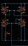
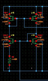
I see that the biasing circuit below is used a lot in op amp design. However, I couldn't find any document explaining how it works. Could anyone tell me some document explain the operating principle of the biasing circuit?
Or could you explain it to me?
Thanks.

attachment.php
 

Attachments

  • biasing circuit.JPG
    biasing circuit.JPG
    25.3 KB · Views: 206

No, this is a CMOS PTAT (delta-VT) current loop, similar
to what you'll find at the core of a BJT based bandgap.
Your operating principle is that there's a single current
point where Vgs_m=4(I)+I*40K=Vgs_m=1(I), and the
mirror loop will lock to it (assuming it starts at all).

Beware the starup issues, since there is no explicit
startup circuit evident, and a relatively poor HF PSRR
as a result of weak unbuffered P and N current ref
rails.
 
  • Like
Reactions: anhnha

    anhnha

    Points: 2
    Helpful Answer Positive Rating
Thank you very much for the explanation!
I think the top 4 mosfets is the improved Wilson current mirror that ensures the current at two branches are equal.
Is that right?
And could you suggest a better biasing circuit that is good as power supply voltage varies a lot and maybe, temperature also changes?
 

Status
Not open for further replies.

Part and Inventory Search

Welcome to EDABoard.com

Sponsor

Back
Top