Continue to Site

Welcome to EDAboard.com

Welcome to our site! EDAboard.com is an international Electronics Discussion Forum focused on EDA software, circuits, schematics, books, theory, papers, asic, pld, 8051, DSP, Network, RF, Analog Design, PCB, Service Manuals... and a whole lot more! To participate you need to register. Registration is free. Click here to register now.

Bandpass matching circuit design for wideband LNA

Status
Not open for further replies.

Ata_sa16

Full Member level 6
Joined
Mar 29, 2016
Messages
343
Helped
59
Reputation
118
Reaction score
58
Trophy points
28
Location
Milky Way Galaxy, 179° 56′ 39.4″
Activity points
2,221
Hi people,

I want to understand how I can calculate parameters for this band pass matching circuit.

If you have any source about matching circuits like this, can you send it to me please.

Matching is done in frequency band of 3-5 GHz and the input network belongs to input equivalent resonant circuit of LNA.

my questions are:

1) why this topology is used, generally Pi or T circuits are used for band-pass matching.
2) How can I calculate this circuit parameters.

For example should I find the input Zin and try to match it to 50 ohm is 4 GHz !??!!? matching.png
 

One factor is reactive impedance. You need to select L & C values which cooperate with current levels running in your circuit. Another way to express it is the L:C ratio.

At a given frequency, the smaller Henry value shows small impedance as compared to a large Henry value. The smaller C value presents larger impedance.

If you need a bandpass which also blocks DC, then a series LC is appropriate. Again you must choose L & C values which pass the desired current level.

- - - Updated - - -

L:C ratio also affects bandwidth. By running simulations you can explore the various effects. In each coil, it's a good idea to install some amount of ohmic resistance. Because, if there is no resistance, then Q soars to unrealistic levels, causing the simulation to mislead us.
 

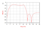
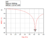
I substitute the inductance models with Real ones including their Q. I set the Q to 50 since it is off-chip external circuit.ac.pngs11.png

This is my simulation results:

S11 parameters is quite precise and correct. But when I check AC simulation from input to output I obtain the figure below.
The Band-pass filter is supposed to have pass band of 3-5 GHz; however, it gives different AC response.
 

Band-pass Matching Circuit is absolutely used but you did a mistake.
Parasitic elements can not be inserted as you have done.And their values are pretty high as I see.
 

Status
Not open for further replies.

Similar threads

Part and Inventory Search

Welcome to EDABoard.com

Sponsor

Back
Top