crazyfox
Junior Member level 2
bandgap reference
HI :
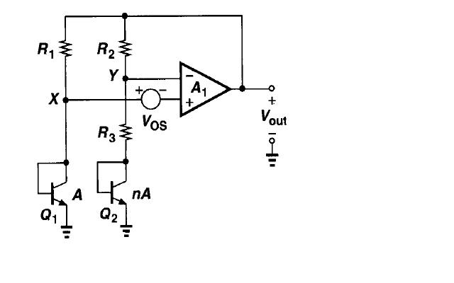
I am trying to design a bandgap , and the topology is like below ,
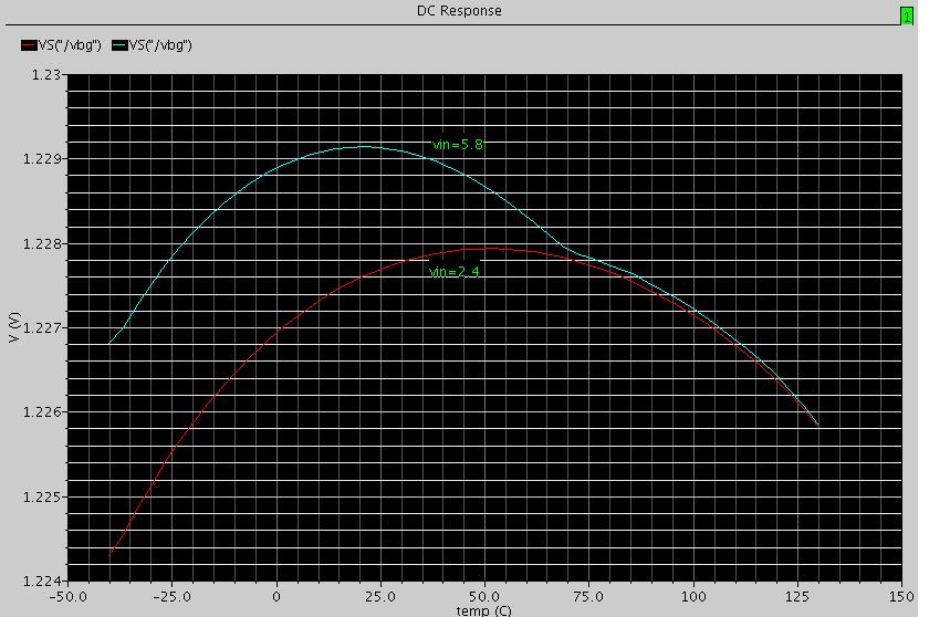
The supply voltage is between 2.4 to 5.8 (v) , and i use .6um process
The temperature is vary from -40 to 130 degree
The opamp that i used has 75 (dB) gain and 60 phase margin
My question is that, when the supply voltage is larger the curve like below
seems not correct, but i have sure that the output stage has enough drive
current, and opamp gain and phase margin is enough .
Can anyone give me some suggestion that any thing i didn't concern?
Thx!


HI :
I am trying to design a bandgap , and the topology is like below ,
The supply voltage is between 2.4 to 5.8 (v) , and i use .6um process
The temperature is vary from -40 to 130 degree
The opamp that i used has 75 (dB) gain and 60 phase margin
My question is that, when the supply voltage is larger the curve like below
seems not correct, but i have sure that the output stage has enough drive
current, and opamp gain and phase margin is enough .
Can anyone give me some suggestion that any thing i didn't concern?
Thx!