Continue to Site

Welcome to EDAboard.com

Welcome to our site! EDAboard.com is an international Electronics Discussion Forum focused on EDA software, circuits, schematics, books, theory, papers, asic, pld, 8051, DSP, Network, RF, Analog Design, PCB, Service Manuals... and a whole lot more! To participate you need to register. Registration is free. Click here to register now.

Balun Impedance design in PCB layout

Status
Not open for further replies.

zzm_3392

Junior Member level 2
Joined
May 15, 2006
Messages
21
Helped
0
Reputation
0
Reaction score
0
Trophy points
1,281
Activity points
1,452
Dear all,
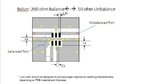
I am confused with the routing of WE748422245 Balun balanced port impedance. Based on the datasheet, I should design proper line width to provide impedance matching. So the balanced port routing is designed by differential 200 Ohm or by single 100 Ohm. It seems the single 100 Ohm from the datasheet.
Furthermore, the PCB is 4 layers, and the critical line is on the top layer, the reference is Midlayer1. The designed 50 Ohm line refers to the following picture. But there is not suitable line width for differential 200 Ohm. Because the line is too small. Can anyone give me some layer stackup suggestion and the corresponding line widths?
Thanks very much.
 

Attachments

  • Balun Impedance.JPG
    Balun Impedance.JPG
    21.5 KB · Views: 159
  • 50 Ohm.JPG
    50 Ohm.JPG
    48.7 KB · Views: 99

I think it's a test board to examine the s-parameters of the balun.The input transmission lines are also 50 Ohm to able to match 50 Ohm connectors.Because there isn't 100 Ohm coaxial connector, instead 50 Ohm connectors have been used.After measurements, obtained s-parameters can be checked in a linear simulator to verify the perfomance of the balun.
In application, the transmission lines must be 100 Ohm to match to the source without connectors.
 

Hi BigBoss,
The transmission lines must be 100 Ohm. Does it refer to single 100 Ohm? If i design a differential 200 Ohm transmission lines, is it ok?
Furthermore, I am design a 4 lyaer's PCB. Please seen the following my designed stackup. For 50 Ohm, the line width is 0.1835mm. But for single 100 Ohm or differential 200 Ohm, the line width is too small, so the stackup is not suitable. Can you give me some suggestion about it? Thanks.
Stackup.JPG
 

Hi BigBoss,
The transmission lines must be 100 Ohm. Does it refer to single 100 Ohm? If i design a differential 200 Ohm transmission lines, is it ok?
Furthermore, I am design a 4 lyaer's PCB. Please seen the following my designed stackup. For 50 Ohm, the line width is 0.1835mm. But for single 100 Ohm or differential 200 Ohm, the line width is too small, so the stackup is not suitable. Can you give me some suggestion about it? Thanks.
View attachment 74152

Yes, for 200 Ohm differential source, you should use 2x100 Ohm single ended transmission line for each input.You can imagine that you cut the generator by 2..
Which layer is used as GND ?? 0.1835mm is also pretty narrow for 50 Ohm line.
Why don't you use standard FR4 with er=4.4-4.7 with 1.6mm thickness??
 

Hi Bigboss,
Thanks your suggestion. The midlayer is uesd as GND. If design was based on 2x100 Ohm single ended transmission line for each input, I worried about whether the two single ended transmission line would be affectd by each other. Because there is a parallel inductor with 0402 footprint between the two inputs, and the gap between two single ended transmission line is less than 0.3mm. Therefore, is it more resonable for design based on 200 Ohm differential source and not 2x100 Ohm single ended transmission line?
For your suggetion about FR4 and 1.6mm thickness, i will try.
Thanks very much!
 

Status
Not open for further replies.

Part and Inventory Search

Welcome to EDABoard.com

Sponsor

Back
Top