Continue to Site

Welcome to EDAboard.com

Welcome to our site! EDAboard.com is an international Electronics Discussion Forum focused on EDA software, circuits, schematics, books, theory, papers, asic, pld, 8051, DSP, Network, RF, Analog Design, PCB, Service Manuals... and a whole lot more! To participate you need to register. Registration is free. Click here to register now.

Audio amplifier design issues

@kka

Newbie
Joined
Feb 18, 2024
Messages
4
Helped
0
Reputation
0
Reaction score
0
Trophy points
1
Activity points
35
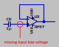
I have to make an audio amplifier with the specifications: Frequency Range: 50 – 20KHz, output voltage : 20mV to 50mV and can be used with 5V supply speaker (8ohm resistance; 0.5W). I made 4 stages first is a preamp stage which has differential amplifier with current mirror load, second stage is a CE amplifier, third is a buffer and 4th is bandpass filter. now i want to add a power amp stage using TIP 31 and 32 power transistors so that I can get required wattage by getting appropriate current gain in this stage but it isn't working. also the output of the 4th stage is 6V(which is fine because designing it on hardware will reduce the voltage gain anyways so I put a little higher gain) but it has a dc offset also there is distortion(uneven) where the sinusoid is of greater amplitude on negative side whereas it is exactly 6 on the positive side. I'm attaching the ltspice file which contains my design and also the image of the output.
Screenshot 2024-02-18 231630.png
 

Attachments

  • draft.zip
    1.6 KB · Views: 68
Your sine-shape appears excellent. The amplitude difference between positive and negative peaks is insignificant (only 1 or 2 percent). This implies your output stage is made from a pair of carefully matched transistors, NPN & PNP.
 
Your sine-shape appears excellent. The amplitude difference between positive and negative peaks is insignificant (only 1 or 2 percent). This implies your output stage is made from a pair of carefully matched transistors, NPN & PNP.
The sinusoid starts differently. Why does it have an offset? Is there something wrong with the way the circuit is biased? Also I want you to help me make an amplifier with necessary current gain using TIP transistors. I'm unable to make one as it doesn't really give the required gain.
 
Your circuits probably contain one or more components which take a few milliseconds to reach normal running conditions, after a signal is applied. Example, power supply. Example, capacitors in a bandpass filter. This sort of behavior is inherent in electronics. That is, an incoming waveform affects the circuitry it travels through.

As for biasing, NPN transistor frequently is uppermost. Whatever amount of voltage swing you desire at output, is the same voltage swing you must bias the NPN.
The voltage gain must come through upstream stages of your amplifier.
 
I'm planning to make a class AB amplifier using TIP transistors(power transistors). Will that work fine? I need a current gain from that. Also please help me with the biasing needed to do that
 
Have you been taught how to analyze the 741 yet? Although this design is old it still exists because it still works even though technology has improved.

I suggest you review how to bias a differential cascode and compare your differences.

If your input bias current is too high, it affects input offset, impedance loss, frequency response , gain and output offset.
U3 has no input bias R and causes your offset and you only need 1 buffer not 3 Op Amps AC coupled.

Do you have any expectations for design specs to verify later? This is important to define using examples. This is how you learn to design.

I am terrible at spelling but I do try to make my schematics readable.

UA741 internals from Falstad site.

1708358525217.png


Compare your pre-amp.
1st stage has no voltage gain and excess current compared to 741 above and in link here
 
I'm supposed to make the amplifier simple and not complex with lesser number of transistors and capacitors. Also the first op amp is buffer, rest two are active bandpass filter to fit in the frequency range. Also could you please clarify where exactly the circuit is going wrong
 
Why design a discrete front end that has no gain then use an H bias with poor low frequency response but high gain then use 3 Op Amps which can be combined into 1?

First tell us all your assumptions so we know what to expect you want.

Number of components.
Bandwidth -3dB
Zin (single or differential impedance or both)
Zout
Max current out.
Total Voltage gain
Pout pwr
Supply Inputs. (single or dual voltage)

Even a simple resistor has a lot of specifications.
 
Hi,

analyzing your post#1:
I have to make an audio amplifier
School project? There are many thousands of audio amplifier projects. Why not gain information from them?
professional: There are ready made available amplifiers. Why not use one of them?


output voltage : 20mV to 50mV
I guess this is wrong.
50mV @ 8Ohms gives just 300uW.

Also, when working with AC you should give additional informations to V, I, P: We don´t know whether 50mV means 50mV peak, 50mV peak-to-peak, 50mV RMS...
(since the missing informations I calculate as if it was DC)

I made 4 stages first is a preamp
Sadly I can´t see open your ZIP on my tablet..

TIP 31 and 32
For 50mV output they are too big,
For 0.5W you need 0.25A ... then they make more sense...

but it isn't working
it´s useless to tell us "it is not working" without additional informations WHY it is not working, how you tested it, what you did expect ...

output of the 4th stage is 6V
this sounds somehow impossible to me, since before you taked about a 5V supply.

but it has a dc offset
Every amplifier has a DC offset. Some in the microvolts, some in the millivolts, maybe even some volts.(like BTL amplifiers),
You need to tell hom much you expect and how much offset you measured and under which conditions.

****
Post#3:
The sinusoid starts differently.
In post 1 you said the frequency range starts at 50Hz. Thus I guess there is a high pass filter. This filter needs some time to settle. So it´s quite expectable that the DC (offset) moves a little for the first tens of milliseconds. This often is referred as the "power ON plop".

help me make an amplifier with necessary current gain
what do you consider as "necessary gain"? ... and gain at which frequency?
Do you talk about the open loop gain, or the closed loop gain?

I'm unable to make one as it doesn't really give the required gain.
required gain???

Klaus
 
Your parts on the schematic are much too far apart making them appear too tiny to see.
The middle opamp is dead because it is missing a DC input bias voltage
 

Attachments

  • dead opamp.png
    dead opamp.png
    3.6 KB · Views: 37

LaTeX Commands Quick-Menu:

Similar threads

Part and Inventory Search

Welcome to EDABoard.com

Sponsor

Back
Top