Continue to Site

Welcome to EDAboard.com

Welcome to our site! EDAboard.com is an international Electronics Discussion Forum focused on EDA software, circuits, schematics, books, theory, papers, asic, pld, 8051, DSP, Network, RF, Analog Design, PCB, Service Manuals... and a whole lot more! To participate you need to register. Registration is free. Click here to register now.

Atlys Digilent DDR2 MIG

Status
Not open for further replies.

maxlutece

Newbie level 4
Newbie level 4
Joined
Jul 30, 2014
Messages
5
Helped
0
Reputation
0
Reaction score
0
Trophy points
1
Visit site
Activity points
57
Hi !

I'm currently working on a project on FPGA. So I try to store a matrix into the DDR2 memory of my Atlys board but I've encountered problems ...

For the beginning I wrote a program on Xilinx which store 20 data of 32 bits in the memory and after that I tried to read the memory value of those cases on the LED. At each button push I display the next value but the problem is I don't have all the values.

More in details, I used a MIG core for interfacing the memory.The memory part reference is EDE1116AXXX-8E is set at the frequency 333.33 MHz.

The datasheet is available here https://www.xilinx.com/support/documentation/user_guides/ug388.pdf

I think that the problem can result about clocks :

- c3_sysclk_2x and c3_sysclk_2x_180 set to 666.66 Mhz
-calibration clock c3_mcb_drp_clk is set to 83 MHz (should be between 50 and 100 MHz)
-user clock c3_clk0 that is used for command writing and reading is set 333.33 MHz

The read values are not the same when I change the user clock, at 333.33 Mhz I have only a few values. When I read 20 datas the c3_p3_rd_empty is asserted after pushing the reading button 20 times. After reading 5 to 10 datas, I read the same value until the end.

I have set two unidirectionnal ports, p2 for writing and p3 for reading.

I have tried to send data with only one impulsion of c3_p2_wr_en (page 53 of the datasheet) and also with one impulsion for each change of the data (page 55 of the datasheet) but with no result.

I verified that the calibration is done and it's ok.

Do you know a tool to see the content of the DDR2 memory ? It can help me a lot because I can understand if the problem is due to the writing or the reading.

And do you have an idea for the clock configuration ? Maybe mine is wrong

Thank for your attention
 

Did you simulate the design with a testbench berfore implementing it? If not try that first. Did you verify the memory timing constraints were all applied correctly? You could also use chipscope if the simulation works but the implemented design doesn't.

Regards

- - - Updated - - -

It just occurred to me, did you debounce the switch input you are using to start the reads? That might explain the inconsistent reading (assumed), multiple reads occurring for one push of the button.

You're problem description has a lot of information, but most of it is not useful to assist you with debugging this problem. You mention you change the user clock but only discuss the 333.33 MHz case? If you read anything that you wrote the clocks are correct, otherwise you wouldn't be able to read even one value you wrote.

What do you mean by "one impulsion" so you had a single strong urge to send data using c3_p2_wr_en? I think you meant to say that you sent a single clock cycle pulse on c3_p2_wr_en? If so how did you generate this single clock wide pulse? Using the output of your push button?

Regards
 

Thanks for your answer.

Yes I did simulations (see below).
The push buttons are all three used with a "debouncing" block, I tested it.
For the user clock, when I tried with smaller frequencies (100, 200 and 250 MHz) it was almost the same result but there was even less read datas.
"One impulsion" means that the enable signal stays high as long as there are datas to write, with the input data changing at every user clock cycle.

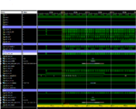
I did some simulations to show you how my program communicates with the DDR2, of course we don't see any response from DDR2 here as it is HW :

1- I load the write FIFO with 25 values while p2_wr_en is high :
LoadWriteFIFO.PNG

2- I push the "btn3" to do the command enable to write the data into the DDR2 at address 00...001 (p2_cmd_en high) with burst length = 25 :
WritingMemory.PNG

3- I push the "btn2" to launch the read from the DDR2 at address 00...0001 with burst length = 25, the data should fill the FIFO of the port 3 (used to read the DDR2) :
ReadData.PNG

4- I push the "btn5" to release the data at the output of the read FIFO and to output the next data (I do this operation several times) :
LoadReadFIFO.PNG

You can see all the important signals I use to drive tis DDR2 memory.
Are this pictures enough to verify the memory timing constraints ? If not what are this constraints ?

The calibration goes well as I put the "calib_done" signal on a LED which is on.

Thank you again for your help.
 

Well posting simulation waveforms are helpful, but how come you have no read data showing up in the simulation? All I see are 1's on p3_rdata[31:0] (I'm not even sure if that is the data coming back from the DDR2 controller, as I have no clue how you've hooked up the DDR2 controller)

As your simulation doesn't show you can write to the DDR2 and subsequently read from the DDR2, how do you expect it to work on the hardware?

Did you get a model of the DDR2 memory you are using and put it in the testbench? I wouldn't know since you haven't supplied any of your testbench or code. (hint, makes it hard to help without have what you have in front of you, i.e: I'm not psychic and if I was I would be buying lottery tickets ;-)).

Regards
 

Thanks for your help ads-ee.

I use simulation just to verify if input signals are properly managed. So I can see like if they are the same like the timing path for writing and reading in the data sheet.

So I don't have any simulation model for the DDR2 memory, I don't find it ... So I cannot obtain any answer from the DDR2. If I can have it, it can be very helpful to understand the DDR2 behavior

Thanks a lot

Kind regards.
 

Grab a model from Micron's web site https://www.micron.com/products/dram/ddr2-sdram#fullPart. Pick something that matches the part on that Atlys board or is at least has similar specs. Add it to your testbench then run the simulation, otherwise the simulation isn't going to help you debug this and debugging it on the hardware is going to be a huge effort and a lot of lucky guessing (if you don't have a chipscope license).

Regards
 

Thanks for your answers

I don't find my memory part on all links. Mine is MIRA P3R1GE3EGF-G8E or EDE1116AXXX-8E.
Maybe if I find another project or simulation which deal with the same memory, I will be able to understand what's wrong with my program.

Regards
 

I'm sure you should be able to find a compatible Micron part, look at the specs of the part on the board and find one that matches from Micron or is at least close, Micron's behavioral models aren't encrypted (at least the last time I grabbed one in Q2 2013) so you could always modify it to match the latencies of the part your using.

Regards

- - - Updated - - -

This appears to be somewhat relevant:
http://forums.xilinx.com/t5/MIG-Memory-Interface-Generator/Atlys-Spartan6-memory-part-MIRA-P3R1GE3JGF-does-not-exist-in/td-p/386495

Make sure you follow the advice given for MIG if you haven't already.

I find it interesting that searching for MIRA doesn't make it easy to find Duetron Electric Corp. Kind of poor marketing for that company in my opinion. If your web presence doesn't show up in the first 5 hits on a web search you should use a different moniker for your company that does show up.

Try typing just micron in a web search box...(1st hit)

Here is a micron part that is also 64M x16:
 

Thank you for your answer
I will try to add in my project a simulation model of Micron which looks like the same as my memory part.
I didn't think it was so difficult to manage DDR2 memory. I thought it was working as well as the block RAM ..

Regards
 

Status
Not open for further replies.

Part and Inventory Search

Welcome to EDABoard.com

Sponsor

Back
Top