nelly1
Junior Member level 3

- Joined
- Jun 14, 2012
- Messages
- 29
- Helped
- 0
- Reputation
- 0
- Reaction score
- 0
- Trophy points
- 1,281
- Activity points
- 1,495
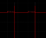
I use two same mos diode(G and D connected mosfet which acts like diode) stacked as normal free wheeling diode. The symbol is like the pic1 below because they are insulated mosfet with pwell/dnwell and dnwell/psub junction diodes.
The problem is
1.when the diode is reversed biased, their voltage drop (VDS) are not the same,whatever the mosfet size is large or small..
2.when i add a VDC=Vth between the G and D of the lower mosfet to decrease the forward voltage drop, (when the diode is forward biased and current is small, Vgs=Vth, Vout=Vin-vth), why the reverse voltage drop of the lower mosfet increase?
REALLY NEED SOMEONE HELP!!!!!!!!!
Attachments
Last edited: