shaikss
Full Member level 4

- Joined
- Jun 18, 2007
- Messages
- 229
- Helped
- 1
- Reputation
- 2
- Reaction score
- 1
- Trophy points
- 1,298
- Activity points
- 3,319
Hi,
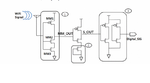
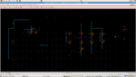
I am designing an ASK demodulator for RFID Tags. I have attached the circuit diagram. This is the ckt from IEEE paper.
If you look at the ckt, the first stage is the inverter kind of thing. I didn't get why second NMOS is used for Stage I. Similarly, the second stage is also inverter with two NMOS. Again, the question is why second NMOS. But when I checked the output of that stage, it is acting like a latch. The last stage is buffer.
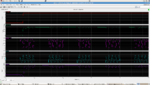
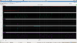
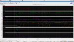
I generated ASK modulated signal and fed as input to the demodulator. I expected that whenever modulated signal is present, demod output is '1' and when no signal is present, it is '0'. To my great surprise, it is always '1'. I tried to give the input by delaying it. So, for the very first time, because of the delay, I could see a logic '0`' at the output. After the delay, there is signal and so the output is logic '1'. Afterwards, though there is no signal, I don't see logic 0 at the output. Its always high. I assumed that the second NMOS at second stage is acting like a latch. Please let me know how can I redesign it? Or Is my understanding wrong? I have attached the simulated results.
I am designing an ASK demodulator for RFID Tags. I have attached the circuit diagram. This is the ckt from IEEE paper.
If you look at the ckt, the first stage is the inverter kind of thing. I didn't get why second NMOS is used for Stage I. Similarly, the second stage is also inverter with two NMOS. Again, the question is why second NMOS. But when I checked the output of that stage, it is acting like a latch. The last stage is buffer.
I generated ASK modulated signal and fed as input to the demodulator. I expected that whenever modulated signal is present, demod output is '1' and when no signal is present, it is '0'. To my great surprise, it is always '1'. I tried to give the input by delaying it. So, for the very first time, because of the delay, I could see a logic '0`' at the output. After the delay, there is signal and so the output is logic '1'. Afterwards, though there is no signal, I don't see logic 0 at the output. Its always high. I assumed that the second NMOS at second stage is acting like a latch. Please let me know how can I redesign it? Or Is my understanding wrong? I have attached the simulated results.