Continue to Site

Welcome to EDAboard.com

Welcome to our site! EDAboard.com is an international Electronics Discussion Forum focused on EDA software, circuits, schematics, books, theory, papers, asic, pld, 8051, DSP, Network, RF, Analog Design, PCB, Service Manuals... and a whole lot more! To participate you need to register. Registration is free. Click here to register now.

anybody has used Diodes Inc AP3503E ?

Status
Not open for further replies.

gtnbng

Newbie level 4
Newbie level 4
Joined
Jul 7, 2014
Messages
7
Helped
0
Reputation
0
Reaction score
0
Trophy points
1
Visit site
Activity points
62
Hi All,

I need a power regulator with Vin=12 VDC, VOUT=5 VDC, Iout=2 A. I guess using a linear voltage regulator for this is out of question.

I found a part in Mouser, AP3503E from DIODES INC.

Datasheet is available here

HTML:
diodes.com/datasheets/AP3503E.pdf

Application notes available here

HTML:
http://diodes.com/_files/products_appnote_pdfs/power/sw_reg/AN1073.pdf

Has anybody used this IC in their design? Is it standing up to the claim?

The IC is small SMD, no special heat removal arrangement, even at the claimed efficiency, it still needs to dissipate about 1-2 W of heat.

Before making up my mind,somebody's experience can be of great help.

Thanks in advance.
 

AP3503E is Buck converter or switching regulator family. It's not a linear regulator.

Proper layout matters. Input and Output loops should be properly routed. 1-2W will not be completely dissipated in IC itself. Buck losses consists of Input capacitor, Output capacitor,Inductor, MOSFET, freewheeling diode and IC quiscent power loss. Mostly Quiscent power loss+ MOSFET power loss+MOSFET Driver power loss will be handled by IC.at 0.7A MOSFET Ron = 100mOhms even with this worst case power dissipation of MOSFET (main component) is 3*3*100mohms = 0.9W .

If you handle the layout properly. You can easily achieve this......

For more through report Refer "Unraveling Buck Converter Efficiency and Maximizing Performance" from microsemi.
 
  • Like
Reactions: gtnbng

    gtnbng

    Points: 2
    Helpful Answer Positive Rating
@malli_1729:

Thank you very much.

I got samples for AP3503E. As I do not have a board for it, I set it up on a perforated board with TH components and an improvised heatsink.

My Vin is 12 V. The voltage output -Vout=5 V and open-circuit FB and COMP and all other signals are perfect. But when I connect to a load of 4 ohms, I get a current of 43 mA , Vout dropping to 0.17 V.

Do you have any idea what should I look at ? I have checked the components and the circuit for short, I find nothing wrong except the noises that may radiate from the legs of TH components.
 

can you post a ruff diagram..... is Open circuit FB and COMP means you are not connecting anything to these pins....
Please design buck as per requirements. Calculate all the components...Post a schematic....
 

Open circuit refers to Vout alone. When Vout is open - not connected to load - then signals on all pins and Vout are correct, but the moment Vout is connected to
a load, the voltage drops to 0.17 V and. I out corresponds to it.

Will post the schematic later.

Thanks


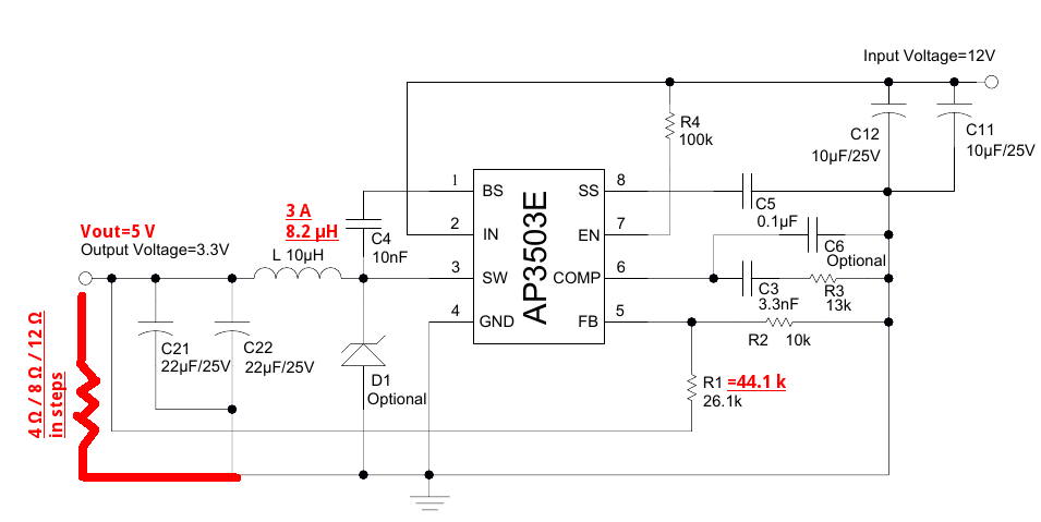
Please see the above schematic. That shows recommended schematic and the changes for my Vout requirement.

I left the circuit on overnight, the Iout (43 mA) is constant, so there is nothing short.

But on load, Vout is dropping and I am unable to get specified Iout
 

I didn't seen any component differences here.... Except C3 recommended is 2.2nF for AP3503E datasheet, but min value is 1.3nF....

Have you seen with different loads like you mentioned 3 loads..try with lower load...whether output is OK.

During this Vout - 0.17V whether it is immediate.. Can u measure Vfb voltage. Whether Input 12V is fine..... I assume all capacitor voltage ratings are taken care and Inductor peak current well above our limit.
 

@mqlli_1729:
I have tried with different loads, 4.5 ohm to 13 ohm. No difference in behaviour.

From your comments, it seems you have used them before. Can you tell me what was your experience ?Did they work for you ?

Thanks,
 

Hi,

what inductor do you use. It sounds to me like a saturation problem.

Klaus
 

During this Vout - 0.17V whether voltage reduction is immediate..?
Can u measure Vfb voltage..?
Whether Input 12V is fine.....?
I assume all capacitor voltage ratings are taken care and Inductor peak current well above our limit... are u sure about this as, KlauST said....
Can u post u r actual wiring diagram.....
 

Have you connected the EP (exposed pad) under the body to GND and some sort of heatsink? It could be that the regulator is reverting to a protection mode when loaded.
Are the capacitors in use low ESR types?
How do you know the inductor should be less for 5V than for 3.3V?
Any application references for the component selection formulas in use?
 

This is the schematic.

7014667300_1405136912.png


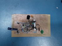
This is the actual wiring on the perforated board,


The white strip is an improvised heatsink for the IC. The pins are projecting out from the sides and wires/components are directly soldered to them.

The inductor is 8.2 µH, 3 A. Saturation does not seem to be a possibility.

Vfb = 0.98 V initially, before switching on the load.After the load is switched on, it is almost zero.

Vin = 12 V all the time.

Vcomp=NIL before load is turned ON, after the load is ON, Vcomp=0.30 V

Vout decreases to 0.17 Volt immediately on LOAD.

All the capacitors are rated for >35V.

The components were chosen based on the recommendation in the Application Notes available on DIODES Inc website [AN1003]. the same document gives formulae to select components.

Thanks all.
 
Last edited by a moderator:

from that Actual wiring diagram...getting details is difficult.....
measure SS voltage with and without load.
If you have DSO can u measure the ripple frequency of your Vout.
Have a switch on EN pin, so that u can control EN pin....

We should know whether IC has encountered any Protections ..like short circuit protection, OVP or Thermal protection.....
 

Hi,

You use electrolytic capacitors. They are not that good for high frequency applications.
In the datasheet usually ther is a section called "..capacitor selection"
There you should find out the specification of the capacitors.

It is not that visible, but ireccomend to use a thick piece of wire for common gnd. Use a star like connection to every device gnd.
Even if not mentioned in the datasheet i'd use a ceramic capacitor with short traces from IN pin to gnd and an additional one at the output signal best directely where the feedback resistor is connected.

About the instability my idea is, that the feedback path sees too much voltage ripple and therefore it shuts dowwn too early with higher load current.
If you want to generate a pcb with solid gnd plane, then i'm sure that you will see improved stability.

There are possibilities to improve stability by connecting capacitors in the feedback path. But this is somehow dangerous, because with wrong values make the circuit to oscillate.

You say the inductivity is rated with 3A. Be sure that this value is named "saturating current" or similar.
What working frequency is the regulator? Is the inductor specified for this frequency?

Klaus
.
 

I've built many SMPS power supplies, and from the photo it does not appear that the inductor, the size of a small 10uF electrolytic capacitor, is designed to sustain a DC bias without saturation.

But I could be wrong. Do you have the datasheet for the component?
 

@all,

Thanks for everybody who enhanced my understanding. The inductor was bought from a local shop, it was sold with that rating, but I am not sure on that.

In the meanwhile I requested and got an evaluation board, the converter works very well.

Looking back, it appears those that doubted the inductor may be correct as the inductor on the EVB is much bigger. The electrolytic capacitors may also have played a supporting role for deterioration.

Once again, thanks all.

The
 

Status
Not open for further replies.

Part and Inventory Search

Welcome to EDABoard.com

Sponsor

Back
Top