Continue to Site

Welcome to EDAboard.com

Welcome to our site! EDAboard.com is an international Electronics Discussion Forum focused on EDA software, circuits, schematics, books, theory, papers, asic, pld, 8051, DSP, Network, RF, Analog Design, PCB, Service Manuals... and a whole lot more! To participate you need to register. Registration is free. Click here to register now.

Protective diodes in FPGA I/O

Status
Not open for further replies.

engr_joni_ee

Advanced Member level 3
Joined
Nov 3, 2018
Messages
750
Helped
2
Reputation
4
Reaction score
4
Trophy points
18
Activity points
6,233
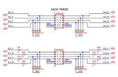
Hi, I just found the attached schematics of ZYBO development board. There are diodes connected to the I/O pin headers. I am trying to understand their role. I guess these diodes only protect the ZYNQ I/O from -ve voltage, for example when the applied signal is negative and goes below the ground level then these diodes will conduct in forward and project the I/O for ZYNQ. What will be the voltage across the diode and the ZYNQ I/O, would it be - 0.7 V ?

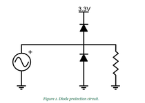
How about protecting the upper end, if the applied signal goes above VCC3V3 ?
 

Attachments

  • Untitled 12.png
    Untitled 12.png
    82.2 KB · Views: 263

If they are Zener diodes they would clamp at Zener voltage. I would guess 3.3V or 3.6V would be used. Zeners still conduct like ordinary diodes in the forward direction so they would still give ~0.6V reverse voltage protection.

Brian.
 

Do you mean, in case the input signal is more than zener voltage, for example 3.3 V than the zener diode will be in reverse bias and will hold the ZYNQ I/O at 3.3 V even through the input signal goes above 3.3 V ?
 

for example 3.3 V than the zener diode will be in reverse bias and will hold the ZYNQ I/O at 3.3 V even through the input signal goes above 3.3 V ?
Within the current rating of the Zener, yes.
A resistor is often used in series with the inputs to limit the current in case the high voltage comes from a low impedance source, such as a power supply.
 

Digilent is using similar protection diodes in a number of eval boards. However without a type specification, it's impossible to predict their effect.

As a general statement, they are probably providing a certain protection against ESD events, but they can't protect the board against longer enduring overvoltage, e.g 5V logic driving the board.
 

It is TVS diode.
Use to protect surge voltage or ESD.
It is not like zenner 100%, equivalent internal resistor is smaller than zenner. That mean it can absorb higher peak power, but voltage clamp is ratio with current.
TVS use for high speed signal or RF (Mhz) will have very low Capacitance and lower peak power.
TVS use for power line protection don't care Capacitance and higher peak power.
Example part#: SMF05CT1G
 

I am working with PCB design that include ZYNQ. I am wondering if I also need to include such protective diode for ZYNQ I/O. There are two options.

1- Use one Zener diode with Zener voltage (Vz) = 3.3 V, the same way I have shown in attached circuit from Digilent ZYBO
2- Use two back to back schottky diode

Which option is better to protect the I/O from over voltage ?
 

Attachments

  • Untitled 13.png
    Untitled 13.png
    13.3 KB · Views: 115

Both will work. Generally, my preference is the two diodes because of the tolerances on Vz and the risk of the dynamic resistance of a Zener allowing the voltage to go a little too high if enough current is available. The penalty is possibly greater capacitance on the signal. In my designs I usually add a high power rated Zener across the supply rails so if any protection diode does conduct and try to lift the supply voltage if can't damage other parts.

As mentioned in post #6, there are specially made low capacitance clamps for exactly this application.

Brian.
 

Hi,
Which option is better to protect the I/O from over voltage ?

It depends:
Example:
A 74HC00 input voltage range is: -0.6V .... VCC+0.6V. Here the double diode is the better option, because during power down it still protects to 0V + 0.6V
A 74AHC00 input voltage range is -0.6V .... 5.5V (independent of VCC) here you may use the zener. You may also use the double diodes.

Btw: you may use double shottky diodes like BAT54S.
There also are multiple line double diode protection devices like IP4220 (including the supply zener)

Klaus
 
Last edited:

Use two back to back schottky diode is good choice for ADC pin of MCU when VADD connect to VDD as same 3v3 as your image.
When apply voltage like 4V to ADC pin, after drop on forward diode 0.4V, it can make VDD rise up 3.3V + 0.3V = 3.6V (event higher if current lower).
Without B2B diode, if MCU switch to another ADC channel, have some problem with ADC measured result. You can test with EV kit. Issue relate to ADC structure (leak between same hold circuit).
If defined pin is use for digital application, TVS is the best choice.
 

The clamp voltage of a 3.3V protection diode is in the range of 5-7 V, please review datasheets. Means they are extending the on-chip ESD protection towards higher energies but are unable to guarantee the maximum ratings of a 3.3V FPGA-IOs.

Forward diode clamps as sketched in post #7 provide a narrower clamping range, but only for current limited signals. They should be used with current limiting resistors and a z-diode to prevent pushing up of the supply rail. You get protection diode array combining both functions:

1644997586655.png
 

Combine is better but make circuit board more complex and size.
Another reason is protection for B2B diode of that pin.
Almost pin of IC have internal B2B diode but limited maximum current can flow through it.
You can see detail some IC will describe about it. Like STM32 MCU, it only accepts 2mA. If any issue make return current higher will spoil expensive IC.
The B2B diode used in this case have to has lower drop voltage compare to internal unit for protection meaning.
 

Hi,

when I read "back to back diode" I have a picture in mind of two diodes in opposite direction.
(Like two people standing back to back looking into opposite directions)

But the protection diodes are in series, both looking into same direction.

Klaus
 

Don't think B2B diode use for clamp ESD because the trace length to TVS clamp diode is too long, and impedance will come high to surge voltage. To protect ESD, surge voltage, TVS/ MOV will place close to where input place, the shortest trace to Power GND for better discharge current.
For price or require lower capacitance, some TVS use multiple B2B diode with 01 TVS clamp diode like image in#11. But this solution make higher clamp voltage as expected.
The rule to select TVS is the stand off voltage, it is same or higher the maximum dc voltage which apply on that net.
For better signal TVS should care it structure (or full detail info), that is why supplier drawn.
 

Status
Not open for further replies.

Part and Inventory Search

Welcome to EDABoard.com

Sponsor

Back
Top