Deepon
Member level 1
jm3395,
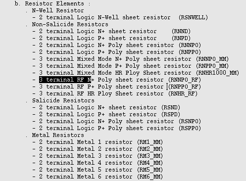
Thanks for the help, but it is a 3 terminal device...
---------- Post added at 15:14 ---------- Previous post was at 14:58 ----------
dgnani,
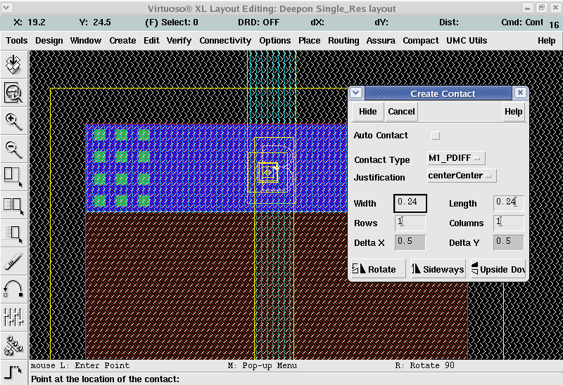
I had tried using the M1_PDiff but it is not completing the net connection..
I wonder if PDiffusion layer will be able to connect with the substrate..
There is something that is bothering me:
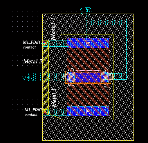
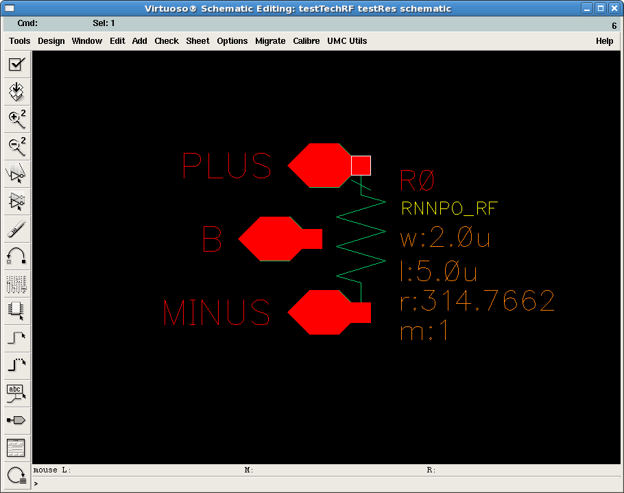
1. In the device level, the 'PLUS' & 'MINUS' terminal contains all the M1 to M5 & there corresponding via contacts placed upon each other.

Then why do I have to again add all the contacts of M1 to M5 on thos terminals in my circuit in order to complete the net connection.
If this can be solved, then perhaps we can decide that why M1_Pdiff is not completing the net.
Thanks for the help, but it is a 3 terminal device...
dgnani -
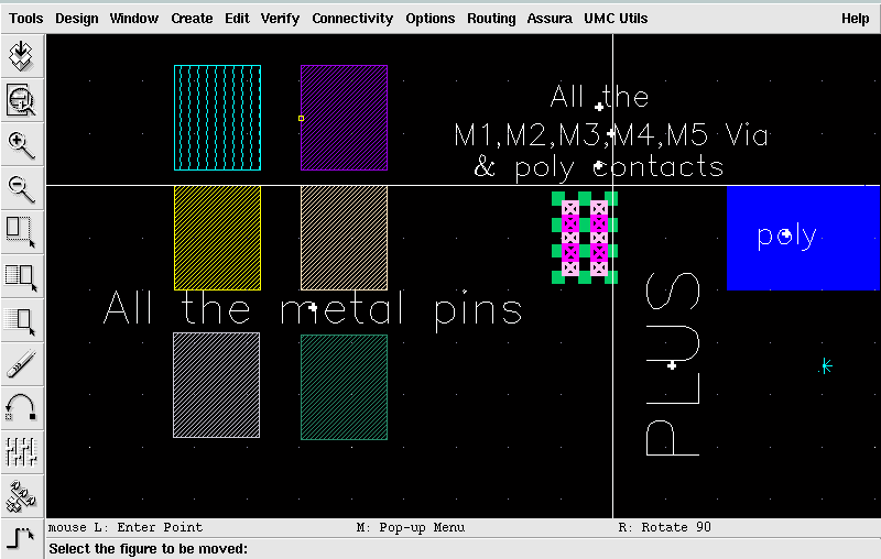
I would agree that the psymbol layer is probably a recognition layer but it is part of the layer construction of the resistor whether it is a real physical layer or not. It was not clear to me whether the "Symbol" layer was indeed the red/orange layer (the label could have been moved to the wrong layer) and if it is just a marking layer, why draw it as big as it is ? Why not draw it as big as the physical resistor ? If the Symbol layer is the red/orange layer and it is a marking layer, why do you need the poly and metal ? The problem is that without the actual data in front of you, you can assume something incorrectly.
In any case, my assumption was that the red/orange layer is a real physical layer that needs poly/metal contacts and not part of the substrate. If I am incorrect, Deepon's answers will tell me that. I am well aware that you do not connect to a substrate with poly. I did mention in my earlier post that you need pdiff to connect to a p-substrate.
It would be helpful to have Deepon respond and clarify things so we can offer helpful advice.
---------- Post added at 15:14 ---------- Previous post was at 14:58 ----------
dgnani,
I had tried using the M1_PDiff but it is not completing the net connection..
I wonder if PDiffusion layer will be able to connect with the substrate..
There is something that is bothering me:
1. In the device level, the 'PLUS' & 'MINUS' terminal contains all the M1 to M5 & there corresponding via contacts placed upon each other.
Then why do I have to again add all the contacts of M1 to M5 on thos terminals in my circuit in order to complete the net connection.

If this can be solved, then perhaps we can decide that why M1_Pdiff is not completing the net.
I am looking at UMC_18 layers and I can tell you that all ?SYMBOL layers are device recognition layers.
You need the poly and metal (and SAB and NPLUS) because those are tapeout layers, necessary for mask preparation.
If you can find an example of physical layers that is not a metal and poly can connect to...
In any case you make a good observation, I had not noticed that there was poly under the B terminals' metal1
This means that those two are dummies (remember this is an RF device) so we still need to connect a p-contact to substrate (should be called something like M1_PDIF).
In summary forget about the previous suggestion of placing p implant rectangles around the B terminal and instead place an M1_PDIF contact (in real RF life you would probably use a guard ring but for now we just want a clean LVS) outside the device perimeter and connect it to gnd! with metal1
This should do the trick
Last edited: