Continue to Site

Welcome to EDAboard.com

Welcome to our site! EDAboard.com is an international Electronics Discussion Forum focused on EDA software, circuits, schematics, books, theory, papers, asic, pld, 8051, DSP, Network, RF, Analog Design, PCB, Service Manuals... and a whole lot more! To participate you need to register. Registration is free. Click here to register now.

[SOLVED] Altium PCB Layout: The Difference of Through Via, Micro Via, and Burried Via

Status
Not open for further replies.

raviani

Newbie level 5
Joined
Jun 6, 2016
Messages
8
Helped
0
Reputation
0
Reaction score
0
Trophy points
1
Activity points
61
Hi, this is my very first time doing 4 layers PCB layout. What is actually the difference between Micro Via and Burried Via? Say I have Layer 1, Layer 2, Layer 3, Layer 4. What I know I use the Through Via for Layer 1 as start layer and Layer 4 for Stop Layer. And how do I use the Micro Via and Burried Via?
Last question, what about the Drill Pair Properties, should I connect every layer there? Thank you so much.
 

You almost certainly do not need buried or micro vias on your first 4 layer board!

Buried vias are vias drilled between some inner layers only, and are an extra process step, on a 4 layer board your inner layers are probably power and a ground plane so you don't have any buried routing layers, and even if you did, adding buried vias is not a cheap option.

Micro vias are vias having very small hole sizes, they are laser drilled and there are strict limits as to how many layers you can penetrate because of aspect ratio limits. You usually use these when trying to fan out a very fine pitch BGA or similar where there is not other way to do it, but by then you are into at least 6 or 8 layers and you will be defining the stackup with layer thicknesses to suit, it is viewed as a high density process with proportionate costs.

For a newbie four layer all vias should be simple full stack, probably minimum 0.3/0.65 or so, and personally I would not tent (Vias make good test points) unless house style calls for it. Vias should not in general have thermal relief (IIRC you need to set a polygon connect rule to make this happen).

Regards, Dan.
 
Thank you so much for your explanation Dan! And what do you mean by 0.3/0.65? Is it 0.3 (drill) and 0.65 (pad)?
 

Just so, hole size/pad size, sometimes you can go to 0.2/0.5 but that will depend on your PCB house, 0.3/0.65 or so is usually doable by most reasonable prototype shops.

Do check the minimums with what your preferred PCB vendor supports, Wurth are very different to a generic Chinese low cost prototype company when it comes to minimum feature sizes for example, it is well worth spending an hour or so setting up design rules.

Note that the 0.3 is the finished hole size, drill diameter is slightly larger.

One other note, set a 0.5 - 1mm keepout around the edge of the board, you don't usually want the internal planes to come right up to the edge, that tends to cause issues.

Regards, Dan.
 
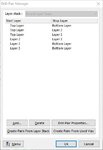
Oh I see.. And what about the drill pairs? Should I do this? Drill Pair.JPG
I am a bit confused about this part also : PCB Rules.JPG
In the Full Query part, should I just write All or should I define every start and stop layers like this : PCB Rules.JPG
 

Status
Not open for further replies.

Part and Inventory Search

Welcome to EDABoard.com

Sponsor

Back
Top