Continue to Site

Welcome to EDAboard.com

Welcome to our site! EDAboard.com is an international Electronics Discussion Forum focused on EDA software, circuits, schematics, books, theory, papers, asic, pld, 8051, DSP, Network, RF, Analog Design, PCB, Service Manuals... and a whole lot more! To participate you need to register. Registration is free. Click here to register now.

Altium - Hierarchical project & buses

Status
Not open for further replies.

szabo.tivadar

Newbie level 2
Joined
Mar 23, 2011
Messages
2
Helped
0
Reputation
0
Reaction score
0
Trophy points
1,281
Activity points
1,306
Hi

I'm facing a weird problem and I don't really understand the error I get. Please help me if you're smarter than me 8)

I create a blank new project, set the net ID scope to hierarchical. This way every net label should be a local one (except power ones). I create 2 subsheets and put a few wires with net labels in them. PA0, PA1, PA2 in the 1st sheet and the same in the second one. No ports, just the main sheet and 2 subsheets, this way there's no connection between the 2 subsheet, compiles w/o errors, so far so good.

I want to put those PAs into a bus: PA[0..2] in both subsheets, however if I connect those wires to a bus and name both buses PA[0..2], the compiler gives me a "duplicate net names bus slice" error. Why? Isn't the bus supposed to be local?

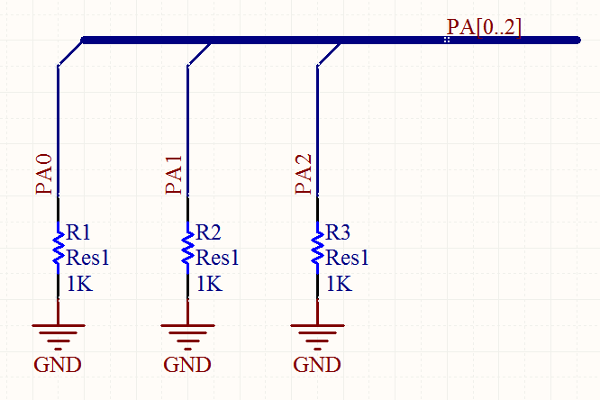
I attach a picture of a subsheet, the other one is the same.

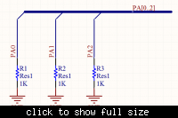
Thank you for your time.
 

I haven't run into that problem but it looks like Altium doesn't want duplicate net names on different subsheets.

From Page 37 of the compiler error reference:
https://www.altium.com/files/Altiumdesigner6/LearningGuides/TR0142%20Project%20Compiler%20Error%20Reference.PDF

This violation can arise when, for example:
• The design is hierarchical, with separate sheet symbols used to reference distinct child sheets, and sheet entries connecting to ports on those child sheets. The Net Identifier Scope is automatically (or manually) set to Hierarchical (Sheet entry <-> port connections). The violation will occur if the same net label has been used on both child sheets. This is because net labels defined on each sub-sheet, even with the same name, remain local to those sub-sheets. The resolution in this case is to ensure unique net labeling is used between sheets.
 
I don't get it. Have a look at **broken link removed**: with hierarchical design net labels should be local. However the explanation you pasted says this is a violation. Now what?
 

My best guess is that they think this is a feature: it alerts you that you have 2 nets with the same name that aren't connected because they are on different sheets with no connection between them. This could get very confusing to debug. I think if you connected the 2 buses together through ports running to the top sheet, the error would disappear.

I agree with you that it isn't what I would expect, those of us with software experience think that local means local, in software it's normal to use the same name (i.e. private int i;) in dozens of routines, and each instance is distinct. But to have 2 distinct nets on the same PCB with the same name is probably a bad idea which could create confusion.


I don't get it. Have a look at **broken link removed**: with hierarchical design net labels should be local. However the explanation you pasted says this is a violation. Now what?
 
I have the same error but I have the two buses connected through ports running to the top sheet. The error does not disapear. I guess net names aren't really local after all
 

I have the same problem as Nolan. I have a top sheet with two sub sheets that are linked with a bus. However, I end up with an error about duplicate net names and it will reference one net in each sheet.

If I remove one of the sheets and put its circuit in the TopSheet, everything works fine. I can't find a tutorial that covers two sheets on the same hierarchical level that are connected with a bus. It is usually connecting sheets vertically.

Thanks for any help!
Jim
 

Figured it out!

Purely syntax. All buses and ports with buses passing through them use brackets [] not parenthesis (); i.e. busname[1..9]. I knew this too, as I had one bus that was fine, I just didn't notice that I messed it up on the bus that I pass from sheet to sheet! I think I messed it up when I used the repeat() command, which uses parenthesis, which got me using parenthesis without thinking about it.

Hope that helps someone.
Jim
 

Hello Jim

I always design my board in PCB document . if my customer need Schematic I draw it separately , that's Because I should deliver PCB in a
specific time . but this time I had a same problem in this project and your solution helps me .

Thank you so much.
 

Hello Jim

I always design my board in PCB document . if my customer need Schematic I draw it separately , that's Because I should deliver PCB in a
specific time . but this time I had a same problem in this project and your solution helps me .

Thank you so much.

Hi Hossein,
can you please advise how you do you pcb without schematics. I also tried doing it but I was advised it is ok for small and simple boards but it is not trustworthy when the board is bigger and complex. can you please let me know how u enter all components and then add netlist to check it against ?
thanks,
keyur
 

Hi keyur
I received an email about your question in Wednesday,and frankly I was very busy.
Forgive me because I check forum Infrequently.
First of all I should tell you I am a reverse engineer.I look at everything from the opposite direction.I learn how to design a multilayer pcb without having schematic.
About your question it is very simpler than it looks.I use Altium Designer and I have some steps after I design my schematics.
The first step called component placement.you don't need to know where you must place your footprints.You should look at your schematic and place components in pcb file(*.pcbdoc in altium designer).The advantage of this step that you can add component when you modify you design or simply delete unnecessary components.I know it is simple in schematic design,but you understand it when you do reverse engineering on a board.
The second and most important and most boring step is netting.In altium you can add nets in pcb but I didn't try the other pcb design software.According to datasheet and your schematic,you should connect your pins to each other and complete your nets.
Now you have nets.you can choose where you should place your components.do this placement part by part and don't do it entirely. you can skip this step and do placement when you route your tracks.
When you did this step, in third step you can just route your tracks.Before routing you should make sure about rules in altium.The most important parts for a small design is "clearance","width","via style"and"polygone" .
After You complete your design you should check it again.In altium it is not a big deal for a small design.This part is necessary because you don't have a schematic file.But I will tell you I did reverse engineering on 8 layer pcbs without having any schematics.I design their schematics after I complete the second step.It is good point to make sure "are your netting is right or not?".You can use "Design rules check" of altium for some errors.
I hope these steps help you but if you have any question I will answer it in this forum.

with respect
Hossein Pirhadi
 
Last edited by a moderator:

I have the same problem as Nolan. I have a top sheet with two sub sheets that are linked with a bus. However, I end up with an error about duplicate net names and it will reference one net in each sheet.

If I remove one of the sheets and put its circuit in the TopSheet, everything works fine. I can't find a tutorial that covers two sheets on the same hierarchical level that are connected with a bus. It is usually connecting sheets vertically.

Thanks for any help!
Jim

I was having the same problem until earlier this afternoon. If you give the bus line a netlabel that is identical to the port than the warnings "Net LabelName has only one pin", and "Duplicate Net Names Element[#]".

Note: I changed "Nets with only one pin" from a No Report to a warning. So my error messages were double what a default setup would give.
 

Status
Not open for further replies.

Part and Inventory Search

Welcome to EDABoard.com

Sponsor

Back
Top