Continue to Site

Welcome to EDAboard.com

Welcome to our site! EDAboard.com is an international Electronics Discussion Forum focused on EDA software, circuits, schematics, books, theory, papers, asic, pld, 8051, DSP, Network, RF, Analog Design, PCB, Service Manuals... and a whole lot more! To participate you need to register. Registration is free. Click here to register now.

Altium designer PCB component display

Status
Not open for further replies.

rocky79

Member level 5
Joined
Sep 20, 2010
Messages
83
Helped
1
Reputation
2
Reaction score
0
Trophy points
1,286
Activity points
1,903
Hello fellows,

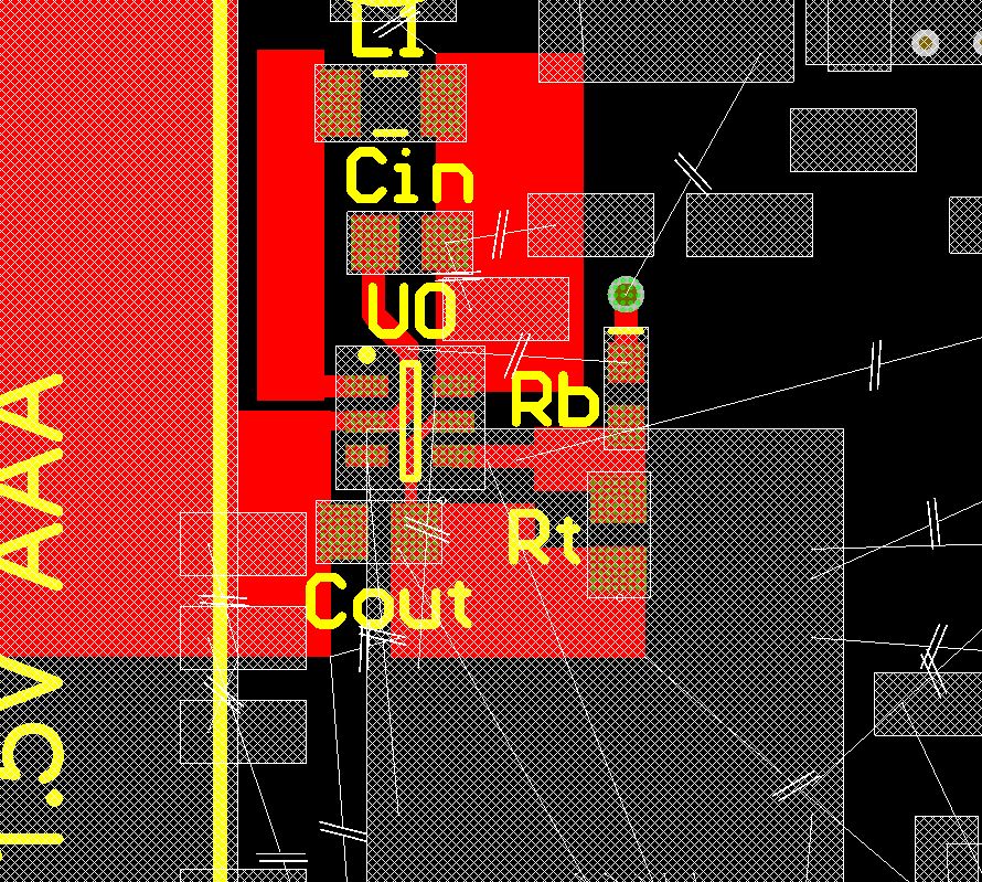
I am having issues turning off the white layer (shown below) in Altium designer and turn on the line connection between various electrical pads. It's quite annoying and i couldn't figure out how to do it. Any idea? Thanks
 

you can manage layers visibility by pressing "L" . also you can manage the line connection by pressing "N"
 

Hi rocky,
You can switch it off & on as follows:
Select Design/Board Layers & Colours->DRC Details Marker...
K.
 

Status
Not open for further replies.

Part and Inventory Search

Welcome to EDABoard.com

Sponsor

Back
Top