Continue to Site

Welcome to EDAboard.com

Welcome to our site! EDAboard.com is an international Electronics Discussion Forum focused on EDA software, circuits, schematics, books, theory, papers, asic, pld, 8051, DSP, Network, RF, Analog Design, PCB, Service Manuals... and a whole lot more! To participate you need to register. Registration is free. Click here to register now.

Altium Designer...How to...

Status
Not open for further replies.

dtvonly

Newbie
Joined
Nov 3, 2014
Messages
2
Helped
0
Reputation
0
Reaction score
0
Trophy points
1
Activity points
17
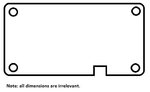
Hi. I have searched the web and youtube but there is no answer to my question. How do I produce a PCB board as in the attached image. Please note that I am new at Altium PCB therefore dimensions are not necessary. I need instructions on how to produce the PCB...rounded corners...cut out for screws...notch for keyed insert. Regards.
 

Attachments

  • altium PCB example.jpg
    altium PCB example.jpg
    16.4 KB · Views: 191

There are several ways to do what you want. What I would do is create the outline of the board on some layer. Then use the command ’Create Board outline From Shape’. (Im not sure of the exact Command, its something like that.) Holes (not ”cutouts for screws”) are just placed like any other component, they're not part of the board outline.
 

Use the line tool to create the outline you desire and then use the define board shape from selected objects option to get the desired board shape. You can use pads for holes, no need to create them in the outline. In the pad properties, use the hole size option to control hole size. Hope this helps.
 

VIAs can also be used for wholes if you edit it properly. But altium price is really what keeps me away from it
 

Status
Not open for further replies.

Part and Inventory Search

Welcome to EDABoard.com

Sponsor

Back
Top