argam
Newbie
Hello,
although I have checked the forum a few times I have never posted, but now I have a few issues that I hope you can help me with.
I am working in a small RF board on Altium Designer. This is my first time using this software and there are a few things I don't know how to do or if they can be done or not.
The board is a two layer board where the bottom layer is ground and the top layer the signal layer. I have also covered the top layer empty areas with a ground plane, placing a polygon plane as it is done in this video:
Altium Designer Tutorial: Copper planes and pours - YouTube
Now I wonder how I can place in an automatic way evenly distributed vias to connect the top ground plane with the bottom ground plane... is it possible to do that or do I have to place the vias one by one??
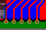
The second question is, the vias I am placing have a cross shape as you can see in the image attached... can I change it so that the vias are connected to the metal completelly?

Finally I am trying to bring the signal lines to the edge of the board so that I can put this board on a larger board and connect both through these "plated edge vias". What I try to do is to end a line at the edge of the board with a via, but having the via in the edge so that only half of it remains on the actual board.

As you can see the last via is half way out, and therefore I will be able to put this board over another board and solder this edge to a pad. Is this done correctly or is there a better way to do what I pretend to do??
Thanks in advance,
Marcos.
although I have checked the forum a few times I have never posted, but now I have a few issues that I hope you can help me with.
I am working in a small RF board on Altium Designer. This is my first time using this software and there are a few things I don't know how to do or if they can be done or not.
The board is a two layer board where the bottom layer is ground and the top layer the signal layer. I have also covered the top layer empty areas with a ground plane, placing a polygon plane as it is done in this video:
Altium Designer Tutorial: Copper planes and pours - YouTube
Now I wonder how I can place in an automatic way evenly distributed vias to connect the top ground plane with the bottom ground plane... is it possible to do that or do I have to place the vias one by one??
The second question is, the vias I am placing have a cross shape as you can see in the image attached... can I change it so that the vias are connected to the metal completelly?
Finally I am trying to bring the signal lines to the edge of the board so that I can put this board on a larger board and connect both through these "plated edge vias". What I try to do is to end a line at the edge of the board with a via, but having the via in the edge so that only half of it remains on the actual board.
As you can see the last via is half way out, and therefore I will be able to put this board over another board and solder this edge to a pad. Is this done correctly or is there a better way to do what I pretend to do??
Thanks in advance,
Marcos.