saeedbayanlou
Newbie level 6
- Joined
- Oct 23, 2011
- Messages
- 11
- Helped
- 2
- Reputation
- 4
- Reaction score
- 2
- Trophy points
- 1,283
- Location
- Tehran, Iran, Iran
- Activity points
- 1,354
Hi everybody
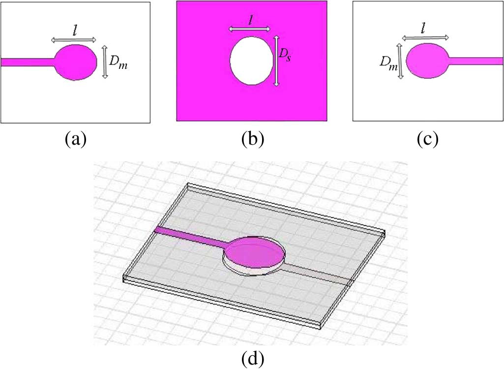
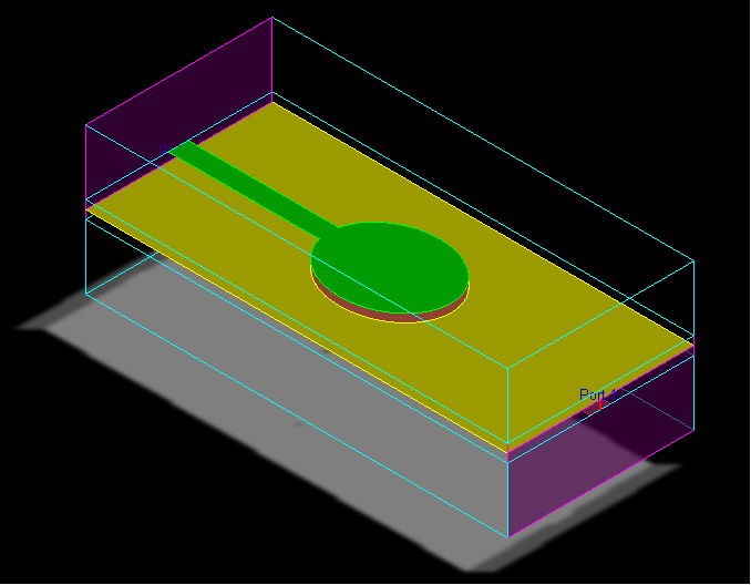
how to draw the attached structure in the ADS layout?
Thanks in advance
how to draw the attached structure in the ADS layout?
Thanks in advance