Continue to Site

Welcome to EDAboard.com

Welcome to our site! EDAboard.com is an international Electronics Discussion Forum focused on EDA software, circuits, schematics, books, theory, papers, asic, pld, 8051, DSP, Network, RF, Analog Design, PCB, Service Manuals... and a whole lot more! To participate you need to register. Registration is free. Click here to register now.

Accumulation PMOS or Depletion NMOS for bypass cap

Status
Not open for further replies.

mtwieg

Advanced Member level 6
Joined
Jan 20, 2011
Messages
3,835
Helped
1,310
Reputation
2,626
Reaction score
1,404
Trophy points
1,393
Activity points
29,363
I've been up on MOS capacitors and am having trouble figuring out the best way to implement high frequency bypass capacitors. It's a simple 5V 0.5um process without triple wells, so some implementations aren't available to me. My top priority is to get maximum capacitance density, but I'd also like to minimize ESR (so poly caps are not an option).

Initially I was planning on using accumulation PMOS with S+G+B tied to Vss and gates tied to Vdd. But someone pointed out that NMOS would have lower ESR due to lower channel resistance/higher electron mobility. But since I do not have any triple well, any NMOS would have to operate in inversion region, and from what I remember from school the high frequency capacitance in inversion is much lower than the depletion capacitance (I need to operate >100MHz). Does anyone know if BSIM models this high/low frequency capacitance difference?

9547238200_1429877585.gif


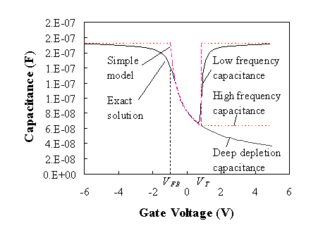
But now that I look at it again, I'm wondering if that's only the case when you have no S/D diffusion areas, only a gate above bulk (who would actually use that?). But if I use an NMOS with S+G+B all tied to Vss, I've read in a couple places that you will see the "low frequency" capacitance even at high frequency. Is this true?

Also on the relative ESR of PMOS and NMOS caps, if the PMOS is in accumulation, doesn't that mean that the charge carriers in the bulk are majority electrons? So shouldn't they have high mobility, just like minority electrons in an inverted NMOS channel?
 

... if the PMOS is in accumulation, doesn't that mean that the charge carriers in the bulk are majority electrons? So shouldn't they have high mobility, just like minority electrons in an inverted NMOS channel?

In case of PMOS (p+) S/D diffusion in n-well you're right: the channel between S & D is in accumulation re. the n-well bulk - so the mirror electrons are majority carriers. But re. the PMOS action the channel is inverted, i.e. there exists a junction between channel and the S/D regions, which prevents a quick supply of electrons, means you may have a good DC cap, but not a good ac cap.

Check this discussion, and these PDFs:
View attachment MOSCAP.pdf
View attachment MOSCAP_voltage_dependency.pdf
 
But re. the PMOS action the channel is inverted
How so? The PMOS is in an Nwell, and the gate is positive, electrons accumulating in an Nwell is accumulation, not inversion.
i.e. there exists a junction between channel and the S/D regions, which prevents a quick supply of electrons, means you may have a good DC cap, but not a good ac cap.
Yes, if you call the accumulated electrons in the Nwell a channel (I wonder if it's okay to use the term for accumulated charges instead of enhanced/inverted charges), then the P+ S/D regions form diodes which would have no bias, so that would block charge transfer (or at least decrease capacitance) to those regions. However, I will also be tying the Nwell to gnd along with the substrate and S/D regions, so the Nwell contacts are another path for the electrons. Will those P+ regions still get in the way then? I guess they would then have to pass through charge-neutral Nwell, which would have a high resistance....

If I remove the P+ regions, then I guess I'm left with a simple AMOS cap. Nothing wrong with that physically, but I don't think Cadence will be able to extract it properly, and LVS would probably throw a fit. Not sure about the foundry...

Thanks, but neither of these seem to address the issue of high frequency response for an accumulation PMOS capacitor? The first pdf only refers to PMOS cap in inversion, the second pdf doesn't refer to frequency response or ESR.
 
Last edited:

Accumulation NMOS in Nwell for RF bypass cap!

The PMOS is in an Nwell, and the gate is positive, electrons accumulating in an Nwell is accumulation, not inversion.
Right, I wrote so: accumulation re. the Nwell. If you regard the PMOS action, however, this is an inversion of its normal behaviour: not a p-channel is built up, but an n+ "channel" - an n+ accumulation region instead of a p+ channel. Perhaps a misunderstanding.


Yes, if you call the accumulated electrons in the Nwell a channel (I wonder if it's okay to use the term for accumulated charges instead of enhanced/inverted charges), then the P+ S/D regions form diodes which would have no bias, so that would block charge transfer (or at least decrease capacitance) to those regions. However, I will also be tying the Nwell to gnd along with the substrate and S/D regions, so the Nwell contacts are another path for the electrons. Will those P+ regions still get in the way then? I guess they would then have to pass through charge-neutral Nwell, which would have a high resistance....

If I remove the P+ regions, then I guess I'm left with a simple AMOS cap. Nothing wrong with that physically, but I don't think Cadence will be able to extract it properly, and LVS would probably throw a fit. Not sure about the foundry...

For a good ac cap you should use an NMOS in Nwell, s. item 5.3: N+ over Nwell gate capacitor in the (p. 5). Such an accumulation cap can quickly supply majority carriers and doesn't depend on the slower electron supply via the S/D junctions or the relatively high-ohmic Nwell bulk.

Extraction and LVS may be a problem. Our process PDK supported such an N+ in Nwell MOSCAP.


Thanks, but neither of these seem to address the issue of high frequency response for an accumulation PMOS capacitor? The first pdf only refers to PMOS cap in inversion, the second pdf doesn't refer to frequency response or ESR.

Yes, I know, not too directly, sorry for that. But the first one tries an estimation of the frequency response of a PMOScap (p. 75 resp. 5 of the PDF), and the second one at least shows the N+ in Nwell RF MOSCAP solution.
 
Last edited:
  • Like
Reactions: mtwieg

    mtwieg

    Points: 2
    Helpful Answer Positive Rating
Re: Accumulation NMOS in Nwell for RF bypass cap!

Right, I wrote so: accumulation re. the Nwell. If you regard the PMOS action, however, this is an inversion of its normal behaviour: not a p-channel is built up, but an n+ "channel" - an n+ accumulation region instead of a p+ channel. Perhaps a misunderstanding.
Okay, different "inversion," understood.
For a good ac cap you should use an NMOS in Nwell, s. item 5.3: N+ over Nwell gate capacitor in the (p. 5). Such an accumulation cap can quickly supply majority carriers and doesn't depend on the slower electron supply via the S/D junctions or the relatively high-ohmic Nwell bulk.

Extraction and LVS may be a problem. Our process PDK supported such an N+ in Nwell MOSCAP.
Yeah the nwell AMOS cap is likely my best bet, if I can get it to work in my process. It's not mandatory that it extract/LVS properly, so long as it actually works. I've been told that it can be implemented, but none of the tools will tell you if you're implementing the layout correctly, and I have no example layouts to go on.

Yes, I know, not too directly, sorry for that. But the first one tries an estimation of the frequency response of a PMOScap (p. 75 resp. 5 of the PDF), and the second one at least shows the N+ in Nwell RF MOSCAP solution.
Right, it's sort of an odd issue to explore. But also odd that my process doesn't accommodate the nwell amos properly since it's obviously useful and can be implemented.
 

Re: Accumulation NMOS in Nwell for RF bypass cap!

... none of the tools will tell you if you're implementing the layout correctly, and I have no example layouts to go on.

Try the layout shown at item 5.3: N+ over Nwell gate capacitor of the above PDF: A square "ring" of N+ S/D diffusion, poly gate slightly overlapping it (as to the rules). Depending on the size, I'd perhaps use a few more poly contacts than shown at the layout image.

In your 0.5µm process you could perhaps even use poly contacts over the gate area, which would further reduce ESR.
 
  • Like
Reactions: mtwieg

    mtwieg

    Points: 2
    Helpful Answer Positive Rating
Re: Accumulation NMOS in Nwell for RF bypass cap!

Try the layout shown at item 5.3: N+ over Nwell gate capacitor of the above PDF: A square "ring" of N+ S/D diffusion, poly gate slightly overlapping it (as to the rules).
My process is ami05 and I'm using the NCSU CDK. Putting poly over Nactive in an Nwell throws a DRC error saying "poly cannot overlap ohmic diffusion." So it thinks I'm making a resistor. I'm not sure if this is a design rule I can ignore. Best I can do without a violation is something like this:


In your 0.5µm process you could perhaps even use poly contacts over the gate area, which would further reduce ESR.
I'm pretty certain that poly contacts can't go above active. Certainly not with MOS transistors, so probably not for MOS capacitors either.
 

Re: Accumulation NMOS in Nwell for RF bypass cap!

I'm not sure if this is a design rule I can ignore.
If you think it's important, you could try and get a waiver from the AMI fab.

Best I can do without a violation is something like this:

If it's a PMOS in Nwell, you should operate it in accumulation: in contrast to my ): PMOScap_in_accumulation.png

Another way would be to use an NMOS cap in p-substrate, to be operated in inversion like a normal NMOS. Here the minority carriers (also electrons) would be provided by the N+ S/D regions.


I'm pretty certain that poly contacts can't go above active. Certainly not with MOS transistors, so probably not for MOS capacitors either.
Right. Only once I've been allowed by waiver to contact poly over active - and for polycaps only.
 
  • Like
Reactions: mtwieg

    mtwieg

    Points: 2
    Helpful Answer Positive Rating
If high frequency is your concern, you might look at layout
styles which minimize the channel resistance (assume this
dominates the sum of Rg+Rds(on)/2 which is your ESR).
I make decoupling MOS caps fingered, over-square (W >>L)
to drive doen the access resistance, I never make a bulk
decoupling cap as a square slab. I also put criss-crossing
Met1 over poly and Met2 over Met1 for some better-HF
upside (even though low-value, it's something).

I'll usually pick something like a plurality of 20/4 fingers
but I never really bother to look at fine optimization. You
could, though, play with L and nf trades with an eye to
areal capacitance (net) and corner frequency.

If you operate in inversion, you have also the channel-
body capacitance in parallel which could add some bulk
C (probably not great quality, but it's there). Assuming body
is one supply and bulk, another. If you used PMOS in NWell
you have actually two junction caps and a MOS cap and
any overlaid metal capacitance (but this may not be as
good for HF decoupling as the NMOS with its lower channel
resistance, despite more C - you'd need to roughly double
C keeping R the same, to have the same corner f, right?
I don't think the junction caps will be as nearly as dense
as the MOS).

But anyway, stack what you've got as tall as you can stand.
MIM over MOS, even, if your technology allows topography
under MIM (and if you have a MIM, which C5 base flow may
not offer).
 
  • Like
Reactions: mtwieg

    mtwieg

    Points: 2
    Helpful Answer Positive Rating
If it's a PMOS in Nwell, you should operate it in accumulation: in contrast to my ): View attachment 116828
Right, the electrons at the oxide interface will be fast, but what's not clear is the path they have back to the negative biased terminal of the capacitor. It can't conduct directly back to the P+ active regions, due to the PN junction there, so it must pass through the Nwell back to the Nwell contacts, which will increase ESR.

If high frequency is your concern, you might look at layout
styles which minimize the channel resistance (assume this
dominates the sum of Rg+Rds(on)/2 which is your ESR).
I make decoupling MOS caps fingered, over-square (W >>L)
to drive doen the access resistance, I never make a bulk
decoupling cap as a square slab. I also put criss-crossing
Met1 over poly and Met2 over Met1 for some better-HF
upside (even though low-value, it's something).

I'll usually pick something like a plurality of 20/4 fingers
but I never really bother to look at fine optimization. You
could, though, play with L and nf trades with an eye to
areal capacitance (net) and corner frequency.

If you operate in inversion, you have also the channel-
body capacitance in parallel which could add some bulk
C (probably not great quality, but it's there). Assuming body
is one supply and bulk, another. If you used PMOS in NWell
you have actually two junction caps and a MOS cap and
any overlaid metal capacitance (but this may not be as
good for HF decoupling as the NMOS with its lower channel
resistance, despite more C - you'd need to roughly double
C keeping R the same, to have the same corner f, right?
I don't think the junction caps will be as nearly as dense
as the MOS).

But anyway, stack what you've got as tall as you can stand.
MIM over MOS, even, if your technology allows topography
under MIM (and if you have a MIM, which C5 base flow may
not offer).

I found **broken link removed**, and did my own simple SPICE simulations of parallel plates with distributed R and C, and found their formulas for minimum ESR to be pretty accurate, and fortunately much lower than I had estimated. For my process a W/L of 10:1 should give an ESR of 63 ohms per finger, which is tolerable. I only have three metal layers, so not much I can do with metal capacitors. My process does not have a special MIM cap, but does have a poly2 layer for poly-poly caps. Unfortunately poly2 cannot go over active, so I can't stack that on top of my MOS cap. Too bad, that would be very helpful.

I think I'm going to change all my PMOS accumulation caps to NMOS inversion caps, just to be safe. All of them are biased with >2V, so they should be well into their linear range. The only thing I might have to worry about is increased injection into the substrate, so I'll have to be more aggressive with my guard rings.
 
  • Like
Reactions: ipsc

    ipsc

    Points: 2
    Helpful Answer Positive Rating
Right, the electrons at the oxide interface will be fast, but what's not clear is the path they have back to the negative biased terminal of the capacitor. It can't conduct directly back to the P+ active regions, due to the PN junction there, so it must pass through the Nwell back to the Nwell contacts, which will increase ESR.

Right, that's why I suggested NMOS inversion caps.
 

Status
Not open for further replies.

Part and Inventory Search

Welcome to EDABoard.com

Sponsor

Back
Top