gaom9
Full Member level 4
Hi,
I met a strange question about the inductor layout when doing the LVS.
I am designing a LNA circuit which contains 3 inductors, and I used the PDK which is 1P4M process to generate Layouts of them. The Layout of the inductor is make up by Metal4. And the three inductors are connected out from their ports by different metals, two by Metal3 and one by Metal4.
But there is a strange question come out when doing the LVS.
The three inductors are reported different errors.
The two inductors which connected out from their ports by Metal3 can not be recognized, the one inductor which connected out from its ports by Metal4 can be recognized but its parameters do not match the parameters of SCH (but its parameters are the same in SCH and Layout).
Why?...........................................
Please help me.........................
Thank you.
Best regards!
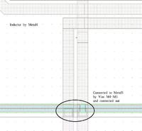
Inductor connected by Metal3
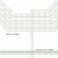
Inductor connected by Metal4
I met a strange question about the inductor layout when doing the LVS.
I am designing a LNA circuit which contains 3 inductors, and I used the PDK which is 1P4M process to generate Layouts of them. The Layout of the inductor is make up by Metal4. And the three inductors are connected out from their ports by different metals, two by Metal3 and one by Metal4.
But there is a strange question come out when doing the LVS.
The three inductors are reported different errors.
The two inductors which connected out from their ports by Metal3 can not be recognized, the one inductor which connected out from its ports by Metal4 can be recognized but its parameters do not match the parameters of SCH (but its parameters are the same in SCH and Layout).
Why?...........................................
Please help me.........................
Thank you.
Best regards!
Inductor connected by Metal3
Inductor connected by Metal4