Continue to Site

Welcome to EDAboard.com

Welcome to our site! EDAboard.com is an international Electronics Discussion Forum focused on EDA software, circuits, schematics, books, theory, papers, asic, pld, 8051, DSP, Network, RF, Analog Design, PCB, Service Manuals... and a whole lot more! To participate you need to register. Registration is free. Click here to register now.

About some strange RF PDK symbols

Status
Not open for further replies.

gaom9

Full Member level 4
Joined
Oct 8, 2007
Messages
228
Helped
7
Reputation
14
Reaction score
5
Trophy points
1,298
Location
China
Activity points
3,294
Hi,
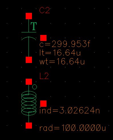
I have a question about the PDK symbols. I used the PDK symbols to make the schematic of an RF design. But I find some symbols are strange as shown in the following figure. In these symbols the CAP and inductor have three pins.
What is the extra pin for? And what should it be connected to, please?

These cap and inductor are for RF design.

Thank you!
Best regards!


15_1215847012.jpg
[/img]
 

Parasitic cap to the shield, usually connect this shield node to ground. For detail value calculation, you can check it in the spice model.
 

    gaom9

    Points: 2
    Helpful Answer Positive Rating
This is the substrate pin or sometimes called bulk pin. It represents a connection pin in the substrate to which the device attached. As stated it is often simply grounded directly or grounded through a substrate resistance component but it can also be used to configure more elaborate device-to-device conduction paths (leakage) through the substrate material.
 

    gaom9

    Points: 2
    Helpful Answer Positive Rating
Status
Not open for further replies.

Similar threads

Part and Inventory Search

Welcome to EDABoard.com

Sponsor

Back
Top