bosskardo
Junior Member level 2

- Joined
- Mar 20, 2014
- Messages
- 24
- Helped
- 0
- Reputation
- 2
- Reaction score
- 0
- Trophy points
- 1,281
- Activity points
- 1,466
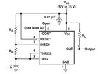
Hi, I saw this sch on NE555P datasheet (https://www.ti.com/lit/ds/symlink/sa555.pdf):

But I've only seen it done like this:

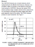
I don't get why the first one is like that. Why is there a capacitor from the power source to gnd? And whats the point of R_L from output to power(I don't know much about 555 internals but could it be that its just opposite to NE555N and I've used NE555N and thats why they are different?)?

But I've only seen it done like this:

I don't get why the first one is like that. Why is there a capacitor from the power source to gnd? And whats the point of R_L from output to power(I don't know much about 555 internals but could it be that its just opposite to NE555N and I've used NE555N and thats why they are different?)?


