Continue to Site
Follow along with the video below to see how to install our site as a web app on your home screen.
Note: This feature may not be available in some browsers.
 .
.Hi all
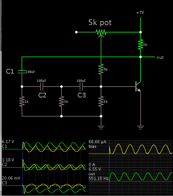
I want to simulate a simple oscillator, which is attached, by hspice, but the output does not oscillate.
please help me to set R,C and W/L in 350nm.
Many thanks
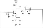
I suggest you use a transistor instead of a mosfet.
The circuit has no DC feedback, so you can cut the loop, place a voltage source at the gate and measure the voltage at the resistor beneath the gate terminal.How to assign loop gain by hspice?
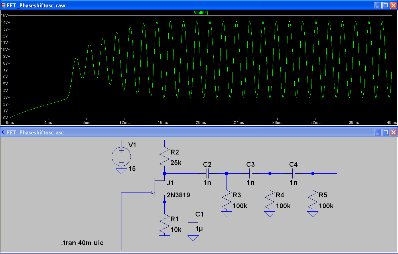
By using equal resistors for R2 and R6, the amplifier gain is already below unity, oscillation is simply impossible. In addition, the oscillator needs some kind of kick-start, as mentioned in post #2. I'm doing it with the "skip initial transient solution" option (uic).my hspice file with Jfet is as follows
I agree with Brad that implementing sufficient gain with a FET can be tricky, it's however possible. I made an example with a JFET in LTSpice.
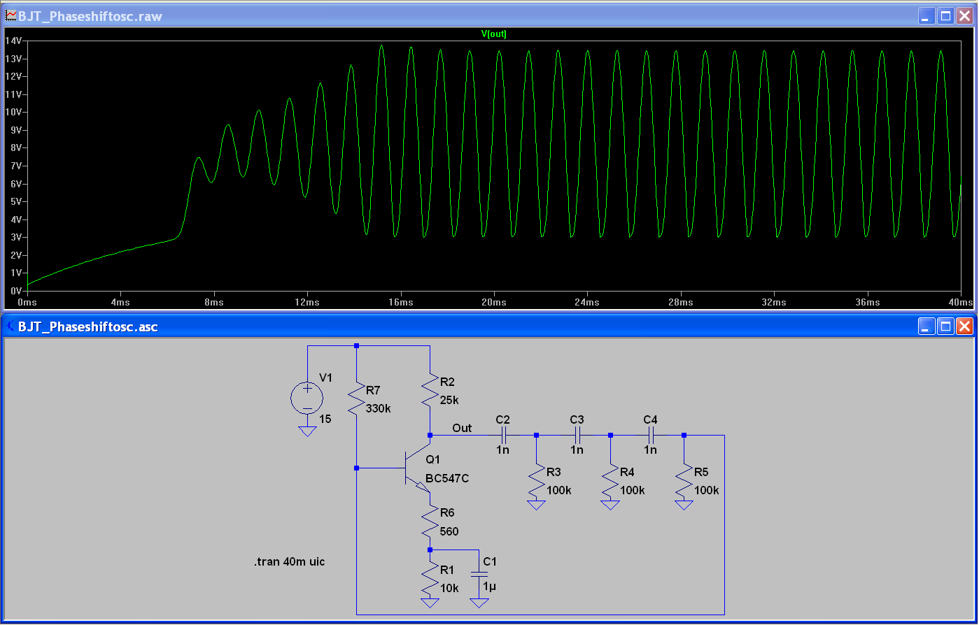
Another question for BJT plz, how to simulate previous circuit by BJT? what's the amount of C and R?
That's possible of course. In the shown circuit, you can create a phase leading effect by placing a smaller source bypass capacitor which also reduces the required amplifier gain.If it is a problem to provide a gain of -29 with the FET, why not using 4 C-R sections (instead of three)?
In this case, the required gain is reduced to (approximately) -18.
Another question for BJT plz, how to simulate previous circuit by BJT? what's the amount of C and R?