Continue to Site

Welcome to EDAboard.com

Welcome to our site! EDAboard.com is an international Electronics Discussion Forum focused on EDA software, circuits, schematics, books, theory, papers, asic, pld, 8051, DSP, Network, RF, Analog Design, PCB, Service Manuals... and a whole lot more! To participate you need to register. Registration is free. Click here to register now.

380V to 18V buck converter, troubles simulating

Status
Not open for further replies.

Unsureofwhattodo

Junior Member level 2
Joined
Dec 21, 2013
Messages
23
Helped
0
Reputation
0
Reaction score
0
Trophy points
1
Visit site
Activity points
234
Hey all, just joined. I'm sorry if this is posted in the wrong section.

Been trying to get a 380V to 18V buck converter designed that can supply up to 4.5A on the output. I'm using a TL494, and I have a TC4452 IGBT gate driver but I'm not sure if I really need it. I can simulate the TL494 by itself, and simulate it along with the TC4452 to get an output square wave with whatever duty cycle/output voltage I want. However, when I implement this with a simple IGBT buck converter, my simulations don't work. I've tried placing feedback into the TL494 in order to keep the IGBT switching, but I just feel lost as to what I'm doing wrong. I feel like the emitter of the IGBT needs to be tied back into the gate, but again it just wiring it together or through a resistor doesn't work.

The picture that's uploaded with this post is a schematic of the 32-12V I've tried to implement instead. I figured if I could get a smaller version to work, the bigger one would just require some value changes.

Edit: I'm not against using a MOSFET in place of the IGBT, the one I have available is the IRFZ34. But I'm still lost as to how to drive a MOSFET switching buck converter.

Thanks for all the help, 32-12v.PNG
Unsureofwhattotdo
 
Last edited:

You certainly do need a driver, just not the one you selected. ;-) If you look at the data sheet you will see that the gate voltage has to be at least 15V higher than the emitter to fully turn on that IGBT (look at the Vce(sat) test conditions). That means you need a gate driver that can supply at least 395V for an input of 380V (since the emitter goes to 380V when the IGBT is fully ON). Neither the TL494 or the TC4452 can provide that. Look at one of these bootstrap drivers for example.
 
Crutshow,

Thanks for the quick reply. I had a sinking feeling after doing some further research that this was the case. Would this circuit be salvageable with a MOSFET in place of the IGBT, or is the design just sunk?
 

Crutshow,

Thanks for the quick reply. I had a sinking feeling after doing some further research that this was the case. Would this circuit be salvageable with a MOSFET in place of the IGBT, or is the design just sunk?
A MOSFET has similar drive requirements as the IGBT so that won't help you.

So why can't you use a high voltage driver as I suggested?
 

Sadly I'm pressed for time. I have until Monday to get at least a 32-12V buck converter working and perform some load testing on it. The original goal was 380-18V, but even if I could design it, I'm not in a position to test it, hence the 32-12V. I figured if I could get a smaller version working, building one with a high voltage input would just require some value changes.

Edit: I need to use the tl494 as my PWM as well, that's part of the project.
 

I have a multitude of MOSFETs ranging from 50V to 500V, a coupleof NPN BJTs (2n3904, fairchild semiconductor), a few of those 600V IGBTs.
 

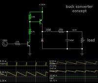
Well, here's a simulation for a discrete bootstrap driver that should get you through the initial testing. With the 2N3904 there is about a 2µs turn-on delay but the regulation feedback loop should compensate for that. It should work for most IGBTs or N-MOSFETs.

But you will need to get a high voltage driver if you want to operate from 380V.

Edit: V1 is the drive from the TI494.

Bootstrap Driver.gif
 
I thought I understood what was going on at first glance, but then I noticed there wasn't an inductor in the schematic. I was under the impression that you needed one in order to buck a voltage down. I see that the circuit gives 4.5A out across Rload with only a 5V pulse to drive the circuit (along with the 16V dc source). I see you've shown me with the second graph Vgs with the Vgate - Vout. I guess my question is two-fold; why isn't there an inductor? and does this buck, if so how?

Thank you so much for everything you've done for me tonight!
 

I neglected to mention that resistive load shown is just for simulation purposes. The load, for a buck regulator, would be the inductor and free-wheeling diode, along with an output load.

Here's a simulation with the inductor and diode. There is an overshoot and oscillation due to the output LC resonant circuit. That will not occur with a properly compensated feedback circuit.

Bootstrap Driver.gif
 
Last edited:

So I've plugged that in to PSPICE (before I saw that you added the simulation) and my results don't match yours. The amperage I'm getting at the output isn't the same, although I do get 16V at the output. I've attached the pictures of the circuit and the output waveform of the current.

Also I tried to move forward with the circuit by replacing the 0-5V function generator with the TL494 to drive the BJT, but alas, I think I'm not driving the BJT properly, or the feedback isn't being done right. The schematic is also attached for you to take a look at.

Part1.PNG
Part1 Graph.PNG
Try #2.PNG
 

My load is 4Ω, accounting for the difference in current.

The signal polarity may be the wrong phase from the Tl494. Note that the output from my driver is ON when the input is low. If you connect the emitter of the TI494 output transistors to the driver input and the collectors to the plus supply, the TI494 output phase will be inverted. See if that works.
 

Tried swapping like you said, so it looks like below now. Still nothing on the simulation. A lot of devices fail to converge.

Try#3.PNG
 

This is a method to drive a P-device at the high side.

The command pulse (at left) is 5V.

Both transistors must withstand 380 V.

Not sure if it is guaranteed to work properly with your control IC.


So are you getting error notices about convergence errors? Those can be difficult to fix. One thing that sometimes work is to go into the simulation limits (Abstol, Reltol, etc.) and reduce the accuracy of each by say a factor of ten.
 

I would try that, but after looking at the voltages/currents that aren't converging, I noticed this.

These voltages failed to converge:

V(X_U3.xinsttl494.58) = 58.85KV \ -33.57V

These supply currents failed to converge:

I(X_U3.xinsttl494.Ev103) = 22.76nA \ -54.49pA
I(V_V2) = -4.053mA \ -4.044mA
I(V_V3) = -775.26mA \ -773.48mA
I(X_U3.xinsttl494.VV51) = -1.236mA \ -1.200mA

These devices failed to converge:
D_D3 X_U3.xinsttl494.DD86 M_M2 Q_Q4


After noticing that one node is somehow reaching 58KV. I'm not extremely adept at using PSPICE, how do I find out which node/pin this is? X_U3 is the TL494 in my schematic.

I've been looking at examples of the TL494 being used to drive BJTs, specifically the circuit linked. How would the wiring change if I had a NPN BJT like I'm using? I'm also curious as to the 47 ohm and the 150 ohm resistors and their role in the circuit. I feel like this circuit could be easily adapted in order to fit my needs, or am I wrong?

httpimg142.imageshack.usimg1424660fig2fy8.jpg
 
Last edited:

I've never found it very useful to determine which node is not converging since there's generally nothing you can do to that node to help.

Another thing to try is to ramp the power supply voltages (I think that's a simulation option), also try skipping the initial DC operating point calculation.
 

Skipped the initial calculations, the insane voltage spike wasn't there in the errors this time. I couldn't find the option to ramp the voltage supplies however.
 

This is a method to drive a P-device at the high side.

The command pulse (at left) is 5V.

Both transistors must withstand 380 V.

Not sure if it is guaranteed to work properly with your control IC.

Note that the 4.7KΩ resistor is dissipating over 30W when the transistors are on. :shock: Of course with a duty-cycle of 18/380 = 4.7% for an 18V output, the average dissipation would be a more manageable 1.5W.

A related concern is that a 4.7kΩ passes only 80mA through the base of the top transistor so the forced gain for a 4.5A output would be 56 which a little high for saturated switching. You typically use a forced gain of 10 with perhaps 20 being an upper limit.

- - - Updated - - -

Skipped the initial calculations, the insane voltage spike wasn't there in the errors this time. I couldn't find the option to ramp the voltage supplies however.
If necessary, you can change the DC sources to a pulse output with a rise time of a ms or so and an infinite (or very long) pulse width to simulate the power supply ramp.

Did you try reducing the simulation parameter tolerances?
 

Ah, can try the power supply change. And I did, but the differences are much larger than the minimum values most of the currents are off by a few mA but the moment you allow that to be ok the simulation just blows up a later. Kind of like putting off the inevitable.


Also I edited the post above asking about a tl494 that drives a BJT, I apologize if you saw it and haven't gotten around to an answer yet.

Edit: Changed the voltage sources to Vpulses like you suggested. Convergence errors are still there. 1ms rise time, 10s pw.
 
Last edited:

Status
Not open for further replies.

Similar threads

Part and Inventory Search

Welcome to EDABoard.com

Sponsor

Back
Top