Continue to Site

Welcome to EDAboard.com

Welcome to our site! EDAboard.com is an international Electronics Discussion Forum focused on EDA software, circuits, schematics, books, theory, papers, asic, pld, 8051, DSP, Network, RF, Analog Design, PCB, Service Manuals... and a whole lot more! To participate you need to register. Registration is free. Click here to register now.

[Moved]: The Kn and Kp parameter

Status
Not open for further replies.

CAMALEAO

Full Member level 4
Joined
Jul 29, 2016
Messages
201
Helped
2
Reputation
4
Reaction score
2
Trophy points
18
Activity points
1,868
Hi to all,

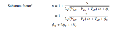
I am trying to get the Kn and Kp from my technology using the methodology that P. Allen describes in his book.

So far I have managed to get those values (there are other parameters that we can get but I haven't tried yet). However there is something strange happening. Well, first the value of Kn is something like 5 times bigger then the Kp. To be more precisely, Kp is aprox. 50uA/V^2 and Kn is aprox. 250uA/V^2.

The question is: Is this normal? From what I have seen in several books and tutorial or lab guides around the web from different universities, where the teachers put the technology parameters, their values are indeed smaller, well the Kp is smaller and more or less smaller than Mine. The Kn is something around 120uA/V^2.

When I try to get the same result by using brute force quadratic equation I get around 500uA/V^2 for the Kn, which is even bigger!

I would like to know if my results, using P. Allen methodology, are reasonable? Or maybe something is escaping from my hands.

Does anyone has tried to do the same?

Regards.
 
Last edited:

Re: The Kn and Kp parameter

Hi erikl, thanks for answer.

Ok, so it means that my results are more or less consistent. The technology is 0.13um and I have use W=L (several ones) and the results were basically the same.

Let me ask you something. This kind of approximation is good only if you are not using low current right? For example, if I want to go to lower currents like 250nA and so on, those parameters will not be the best ones to design anything. I need to extract the Kn and Kp using another methodology, correct? Maybe in here it is best to use the gm/id methodology, no?

Can you recommend a good book to read about sub-threshold operation (is the same as weak inversion correct?)

Regards.
 

Re: The Kn and Kp parameter

This kind of approximation is good only if you are not using low current right? For example, if I want to go to lower currents like 250nA and so on, those parameters will not be the best ones to design anything. I need to extract the Kn and Kp using another methodology, correct? Maybe in here it is best to use the gm/id methodology?
Right!

Can you recommend a good book to read ...
See the book title on the page I showed you above.

... about sub-threshold operation (is the same as weak inversion correct?)
Yes!
 

Re: The Kn and Kp parameter

Ok, thanks. I took a look at this book and it seems to be very advance. Isn't it? What's the book about concretely? Can you recommend the chapters recommended to learn this methodology? And I think they use the EKV model in there. Can this be applied to the BSIM? How?

Do you have any experience either using the gm/id methodology os the EKV model?

Regards.
 
Last edited:

Re: The Kn and Kp parameter

Kn and Kp (k', =u0*Cox) have a sort of standard relation
historically but in technologies like some SOI, strain effects
can alter that relation and may be done on purpose (I have
seen this specifically in RF SOI CMOS technology developments).
5:1 is pretty abnormal.

You may also be seeing the difference between Ldrawn and
Leffective, being "baked into" a model - N and P may have
different deltaL and/or deltaW but maybe for a simple digital
model nobody bothered to extract that because there's only
one channel length of interest (or something).
 

Re: The Kn and Kp parameter

I took a look at this book and it seems to be very advance. Isn't it? What's the book about concretely?
gm/Id methodology

Can you recommend the chapters recommended to learn this methodology?
I remember I studied the whole book, overflying the chapters I thought I already knew enough about.

And I think they use the EKV model in there. Do you have any experience either using the gm/id methodology os the EKV model?
Can this be applied to the BSIM? How?
Starting with the gm/Id methodology you don't need any models, you just need to know - or to measure - the Technology Current of your process, for several transistor sizes and currents, if possible. This is necessary to size the transistors of your circuit. Only then you need the models in order to analyze the circuit.

EKV or BSIM - this depends on availability of models - and if your simulator can handle EKV models.
 
Re: The Kn and Kp parameter

Hi erikl, thanks for your reply and sorry for my late reply.

I took a look at the book in more detail and I have some doubts. Is it possible for you to answer some questions?

The first one has basically to do with one comment that you did in you previous post.

"Starting with the gm/Id methodology you don't need any models, you just need to know - or to measure - the Technology Current of your process, for several transistor sizes and currents, if possible. This is necessary to size the transistors of your circuit. Only then you need the models in order to analyse the circuit. "

When you say Technology current, you are referring to the Io in Binkley's book?

So, like I mentioned, I have read a bit more in detail the first 2 chapters and I have tried to obtain the same results as the ones in the book. From what I have understood he uses some kind of normalised inversion coefficient which is a function of Id and Io as well as W/L and according to him, he does this way to permit a simple design guidance.

He calls it normalised, he's definition because he uses n = n0 which is held fixed at its averaged value in moderate inversion and u = u0 is held fixed at its low-field value. From his comments, this is done to allow normalisation by a fixed current, independent of inversion level - here is where comes one of the question that I had which I did above.

Another question I have here in this comment has to do with the n0 and u0. Where can I get those? To simplify I kinda too n=1.4 just to try something, and using the Id (moderate) I tried to get the u0 by using the equation 3.2 for and W/L = 1. But when I reach the equation 3.5 and I try to get the Io I get the same current I used in 3.2 which is logical. So this way I can't get the u0.

Basically, how can I get the u0? I tried to look to my Mosfet models and basically, it is impossible to get that. If I have identified correctly the u0, I noticed that the u0 had more that 10 variables in which some of them depends on the transistor size.

So how can I get the u0 and the n0?

Regards and thanks in advance.
 

Re: The Kn and Kp parameter

When you say Technology current, you are referring to the Io in Binkley's book?
Yes; actually depicted as I0 .

So, like I mentioned, I have read a bit more in detail the first 2 chapters and I have tried to obtain the same results as the ones in the book. From what I have understood he uses some kind of normalised inversion coefficient which is a function of Id and Io as well as W/L and according to him, he does this way to permit a simple design guidance.

Yes. He simply defines a normalized inversion coefficient IC=1 for a drain current Id of a transistor with (W/L)=1 at Vgs=VT0=UT. This drain current Id is then defined as the Technology Current I0, measured at a so defined IC=1 , in the center of moderate inversion mode.

One could ask which Vds should be used for this measurement. Of course Id=I0 should be in saturation region. Because I found no hint about which Vds to use, in my measurements I use Vds=Vdd/2 .

He calls it normalised, he's definition because he uses n = n0 which is held fixed at its averaged value in moderate inversion and u = u0 is held fixed at its low-field value. From his comments, this is done to allow normalisation by a fixed current, independent of inversion level - here is where comes one of the question that I had which I did above.
I understand your u = u0 is what Binkley depicts as UT (or VT0 in the model files)?

Another question I have here in this comment has to do with the n0 and u0. Where can I get those? To simplify I kinda too n=1.4 just to try something, and using the Id (moderate) I tried to get the u0 by using the equation 3.2 for and W/L = 1. But when I reach the equation 3.5 and I try to get the Io I get the same current I used in 3.2 which is logical. So this way I can't get the u0.
Of course not - it's basically the same equation. Why do you want to calculate u0=UT? This is an adjusted value for the measurement, taken from the model file (VT0), like the low-field mobility value µ0=U0. And as you did, take n=n0 (in the equation) as this average value 1.4 .

Basically, how can I get the u0? I tried to look to my Mosfet models and basically, it is impossible to get that. If I have identified correctly the u0, I noticed that the u0 had more that 10 variables in which some of them depends on the transistor size.

So how can I get the u0 and the n0?

As I told you above: this u0=UT is a value taken from the model file (VT0) to be adjusted for the I0 measurement at a - by this - defined IC=1. For n0 s. above. Or - if need be - take more accurate values - depending on calculations for weak inversion where Vgs < UT (or IC<1), n can get lower values down to 1.3 - or so. You can find a lot of examples in the Binkley book, see e.g. his Figure 3.2 .
 
Re: The Kn and Kp parameter

Hi erikl, thanks one more time for you reply.

About your question:

"I understand your u = u0 is what Binkley depicts as UT (or VT0 in the model files)?"

The u=u0 that I am referring too has to do with the mobility. I should have properly written as µ=µ0. This remark is made on page 51, subchapter 3.4.2.2.

My new questions about your comments:

" Yes. He simply defines a normalised inversion coefficient IC=1 for a drain current Id of a transistor with (W/L)=1 at Vgs=VT0=UT. This drain current Id is then defined as the Technology Current I0, measured at a so defined IC=1, in the centre of moderate inversion mode."

Can you tell me where does he mention Vgs=VT0=UT?

Let me write down a thought on this comment: So basically he defines the current as you mention and assuming that it is like that it means that he gets the current by simulating the transistor under those conditions? Not doing calculations using the expressions that he mentions in the book?
Is that it?

If it is like that I was totally misled. I thought that this was supposed to be calculated based on some physical quantities, like silicon epsilon, tox, cox, and so on.

As I told you above: this u0=UT is a value taken from the model file (VT0) to be adjusted for the I0 measurement at a (...)

I can see the VT0 in my model file, however, it is written in lower case and it doesn't have a constant value, that is, it has a fixed value and some other deltas. Is this normal? Should I take into consideration the whole expression (the deltas) or use simply the constant value and not use the deltas?

Regarding the tox, for example, I have the tox and toxe that according to the BSIM manual is the electrical gate oxide thickness. The last one has some dependence on which corner case you are using. I noticed that the have a significant difference in their values. For the tox should I use the tox or toxe? I was forgetting to mention that there another tox, called toxm which according to the bsim manual is the tox at which parameters are extracted. What does it mean? And by the way, all these parameters, in the model file, are expressed in terms of SI units, correct?

(...) the Binkley book, see e.g. his Figure 3.2.

I took a look at this figure and I read that subchapter. In there it says that the n was calculated and it says that the process have the mentioned parameters. Where did he got the gama (which is the body effect factor) and the phi? Why does he mention the gama if, acording to the n expression on table 3.6 he doesn't use it? Moreover, the n expression depends on itself. How to solve this?

Summarising for now, to get the i0 I should do hardcore calculations or simulations?
 

Re: The Kn and Kp parameter

"I understand your u = u0 is what Binkley depicts as UT (or VT0 in the model files)?"
Sorry, I mixed up this UT designation: With UT Binkley means the Thermal Voltage kT/q=25.85 mV @ T=300K .
The Threshold Voltage is designated as VT.

Can you tell me where does he mention Vgs=VT0=UT?
"=UT" was my error, s. above. He defines VEFF = VGS - VT .

Let me write down a thought on this comment: So basically he defines the current as you mention and assuming that it is like that it means that he gets the current by simulating the transistor under those conditions? Not doing calculations using the expressions that he mentions in the book?
Is that it?
Both is done, I think: As long as you don't have neither a model file nor a transistor, you only can use calculations. From a model file you can extract some parameters which gets you closer to reality, both with calculation and simulation. And with a real transistor, you can get I0 and IC=1 from measurement(s). For their measurement and calculation you need of course VT, either from its model file or from a lot more measurements.

If it is like that I was totally misled. I thought that this was supposed to be calculated based on some physical quantities, like silicon epsilon, tox, cox, and so on.
Right, as long as you have neither a model file nor a transistor.

I can see the VT0 in my model file, however, it is written in lower case and it doesn't have a constant value, that is, it has a fixed value and some other deltas. Is this normal? Should I take into consideration the whole expression (the deltas) or use simply the constant value and not use the deltas?
Model file syntax is case-independent. The fixed values are for typical conditions, i.e. given typ. supply voltage, typ. process and T=25°C (usually). All deltas are given for defined differing conditions.

Regarding the tox, for example, I have the tox and toxe that according to the BSIM manual is the electrical gate oxide thickness. The last one has some dependence on which corner case you are using. I noticed that the have a significant difference in their values. For the tox should I use the tox or toxe? I was forgetting to mention that there another tox, called toxm which according to the bsim manual is the tox at which parameters are extracted. What does it mean?
For calculations and simulations, always use toxe. toxm is from extracted, but not for the given adapted parameters.

And by the way, all these parameters, in the model file, are expressed in terms of SI units, correct?
Right.

(...) the Binkley book, see e.g. his Figure 3.2.
I took a look at this figure and I read that subchapter. In there it says that the n was calculated and it says that the process have the mentioned parameters. Where did he got the gama (which is the body effect factor) and the phi?
Either from the model file (GAMMA, PHI), or from appropriate measurements on silicon.

Why does he mention the gama if, acording to the n expression on table 3.6 he doesn't use it?

Sure he uses it: (γ=GAMMA)

And from page 48:
n is also a function of the body-effect factor, γ, the Fermi potential, PHI = 2ΦF, and the thermal voltage, UT. n increases with increasing γ, corresponding to increased substrate doping concentration and increased body or substrate effect.

Moreover, the n expression depends on itself. How to solve this?
Where did you see this?

Summarising for now, to get the i0 I should do hardcore calculations or simulations?
Depends on what you can get your hands on. See above!
 
Re: The Kn and Kp parameter

Hi erikl,

Alright. So we can get the I0 wither by calculation using the expression that he has in the book or by simulating.

If I want to get the technology current by calculations I need to get the models parameters used in the expression.
If I want to simulate I have to setup a testbench and apply a Vgs = Ut and a Vds = Vdd/2. By applying the Vgs = Ut we are defining the IC as 1?

Now, you say that I have to simulate for different sizes and different currents. Question: How can I simulate forcing a Vds = Vdd/2 and still inject different currents?

Regards.
 

Re: The Kn and Kp parameter

If I want to simulate I have to setup a testbench and apply a Vgs = Ut and a Vds = Vdd/2. By applying the Vgs = Ut we are defining the IC as 1?
Yes, by applying Vgs = VT we are defining IC as 1 . See above. And I think you can read this in Binkley's chapter 3.

Now, you say that I have to simulate for different sizes and different currents. Question: How can I simulate forcing a Vds = Vdd/2 and still inject different currents?

You don't have to inject different currents. At different widths=lengths W=L you will automatically get different currents. Start with W=Wmin, than try W=(3..5..10)*Wmin, always with W=L , so you'll get (slightly) different I0 currents for different W's , as you'll need them in your circuit for further calculations of Id currents at L≠W and/or IC≠1 .
 
Re: The Kn and Kp parameter

Hi erikl,

Thanks for the suggestions. I did what you have suggested but I have some questions about this and others about previous posts above.

Starting with the simulation. I basically put a simples transistor biased with a Vgs = VT0 (taken from the tech file and rounded up) and I have put a source at the drain with a voltage of vdd/2.

I've mantained the ratio of W/L=1 and varied W=L=0.5u, 1.0u, 1.5u, 2.0u and so on. What I've noticed was that the current was increasing with the increasing W and L(maintaining W/L=1). I think this is expected. But if this is expected, I wonder if this the technology current, because I think the technology current shouldn't vary right? Only with temperature. When I say that the current increases, it increase largely, like for example, for 1u/1u to 3u/3u it varies x2,5.

Compared to the expression that we can use to calculate the I0 the result is different.

I don't know if I am doing something wrong.

"You don't have to inject different currents. At different widths=lengths W=L you will automatically get different currents. Start with W=Wmin, then try W=(3..5..10)*Wmin, always with W=L , so you'll get (slightly) different I0 currents for different W's , as you'll need them in your circuit for further calculations of Id currents at L≠W and/or IC≠1."

If I understand you are saying that we will have different current, but like I mentioned above they vary a lot I would say. But even if they didn't vary much,
what you mean by this: as you'll need them in your circuit for further calculations of Id currents at L≠W and/or IC≠1?


Another thing that I have noticed was, I took the VT0 from the model file and I have applied it to the gate of the transistor under test. Curiosly I get a certain
vdsat and a vth which is different from the VT0. Is this supposed to happen? And another thing is depending on the size of the transistor we have different VT0 that can be used. Which one to choose?


Regarding the toxe, you are right, but I have noticed that in the model file the toxe = tox apart from another variable that will depend if you are running corners or montecarlo. So if we want the typical toxe we will land on the tox. Is this the same for you in the model?

Model gamma, I found it. Thanks for the remark.

Regarding the n expression depending on itself, you can see that on the same expression that you have posted. You can see (Vgs-Vth)/n which is odd, right? How can we solve this? Suppose that I wanted to make the same plot as he, in figure 3.2. How that could be possible? Have you tried to do this? What did you get?

You have said that he does some kind of adjustments. Can you point out in the book where he does that? The page with the expressions, etc, please.

Thanks again for the support. Regards.
 

Re: The Kn and Kp parameter

Hi CAMALEAO,
I've mantained the ratio of W/L=1 and varied W=L=0.5u, 1.0u, 1.5u, 2.0u and so on. What I've noticed was that the current was increasing with the increasing W and L(maintaining W/L=1). I think this is expected. But if this is expected, I wonder if this the technology current, because I think the technology current shouldn't vary right? Only with temperature. When I say that the current increases, it increase largely, like for example, for 1u/1u to 3u/3u it varies x2,5.

Compared to the expression that we can use to calculate the I0 the result is different.

I don't know if I am doing something wrong.
No, I think your setup and simulations are ok. I did the same for a 180nm process NMOSFET:
Technology_Current_I0_vs_Channel_Length_L.png
The I0 variation isn't as strong as with your technology - even less than a factor of 2. Only a slight variation as I told you above.


... what you mean by this: as you'll need them in your circuit for further calculations of Id currents at L≠W and/or IC≠1?
Depending on the requirements of your circuit (mainly power consumption and accuracy) you will need transistors with sizes W≠L and/or operation modes IC≠1. How this is needed and done is to be learnt from Analog Circuit Design methods.


... depending on the size of the transistor we have different VT0 that can be used. Which one to choose?
If so, choose that one given for the size of the transistor you use.


... So if we want the typical toxe we will land on the tox. Is this the same for you in the model?
Yes!


Regarding the n expression depending on itself, you can see that on the same expression that you have posted.
I see what you mean. But n does not depend on itself, it's just a second time present in the equation. You could resolve the equation so that n is just once present at the left side of the equals sign, but it would be a little bit troublesome ;-)

You can see (Vgs-Vth)/n which is odd, right?
Where? Why?

Suppose that I wanted to make the same plot as he, in figure 3.2. How that could be possible? Have you tried to do this?
I didn't try this. You need a lot of correct parameters for your process for the calculations, or measurements of gm and gmb to achieve this plot.

You have said that he does some kind of adjustments.
I can't remember that I've said this. If you think so, just show me when and where!

Regards, erikl
 

Re: The Kn and Kp parameter

You have said that he does some kind of adjustments.

I can't remember that I've said this. If you think so, just show me when and where!

See post #9:

CAMALEAO: Another question I have here in this comment has to do with the n0 and u0. Where can I get those? To simplify I kinda too n=1.4 just to try something, and using the Id (moderate) I tried to get the u0 by using the equation 3.2 for and W/L = 1. But when I reach the equation 3.5 and I try to get the Io I get the same current I used in 3.2 which is logical. So this way I can't get the u0.

erikl: Of course not - it's basically the same equation. Why do you want to calculate u0=UT? This is an adjusted value for the measurement, taken from the model file (VT0), like the low-field mobility value µ0=U0. And as you did, take n=n0 (in the equation) as this average value 1.4 .

I will do a big sweep and check when the I0 will start to flatten. But let me comment/ask something.

According to Binkley his technology current is fixed, in this case around 0.64uA. How the simulation that we are doing gives a different values of I0 for each W=L?

If we pick the simulation results for the I0, sSince we will have different values of I0, which one to choose to size the devices?

Best regards.
 

Re: The Kn and Kp parameter

Quick update erikl:

I have simulated the tech. current as you suggested. I swept the W maintaining L=W, from a value near the minimum until something around 100um. The tech. current starts to tend to 820nA after passing the W=L=20um. Curiously the Vth tends to VT0 after the W=L=20um. Before that, it changes like a mentioned above.

What do you think about this?

I will try to do the hand calculations using the expression that Binkley has in his book and see if I can get the same result.

Anyway, if the tech. current is that 820nA, what's the next step then?

Regards.

EDIT: By the way, what do you think of building a spreadsheet with the variables that Binkley uses, then the variables from the model file and from the BSIM manual? Have you done something like that?
 

Re: The Kn and Kp parameter

Erikl, do you use this kind of approach in Binkley book with BSIM models or EKV? Using calculation or only simulations? I am asking this as well because I wonder at which extent can we use, in this case something that was done using the EKV model and maybe with EKV model in mind, in the BSIM model.
 

Re: The Kn and Kp parameter

You have said that he does some kind of adjustments.
See post #9:
This is an adjusted value for the measurement, taken from the model file (VT0)
Ok. But I didn't say that he (Binkley) did some kind of adjustments. Be more careful with such statements, pls.!
Perhaps adjusted wasn't the appropriate word choice, so perhaps led to a misunderstanding. What I wanted to say was that VT (the correct Binkley designation now) hadn't been calculated, but taken from the parameter vt0 from the model file. Compare with my statement above, pls.!


According to Binkley his technology current is fixed, in this case around 0.64uA. How the simulation that we are doing gives a different values of I0 for each W=L?
If you had read/studied the Binkley - or any other Analog Circuit Design - book thoroughly, you'd know the answer: short channel effects as carrier velocity saturation (mobility reduction due to the longitudinal field), CLM and VFMR throttle (pinch, reduce) the drain current most at Lmin, and less and less at longer channel lengths. That's why you get a low I0 value at Lmin and some higher, but more and more saturating I0 values for longer channel lengths.

If we pick the simulation results for the I0, sSince we will have different values of I0, which one to choose to size the devices?
That one for the channel length which you use for a certain transistor in the circuit.

- - - Updated - - -

I have simulated the tech. current as you suggested. I swept the W maintaining L=W, from a value near the minimum until something around 100um. The tech. current starts to tend to 820nA after passing the W=L=20um. Curiously the Vth tends to VT0 after the W=L=20um. Before that, it changes like a mentioned above.
What do you think about this?
I don't know which simulator you're using. With my simulation setup, the Vgs voltage source is kept constant as Vth=VT0 .

Anyway, if the tech. current is that 820nA, what's the next step then?
Use the I0 value appropriate to the channel length you want to use. With this I0 value, either calculate the width W for the required drain current Id, or from a predetermined width W calculate Id.

By the way, what do you think of building a spreadsheet with the variables that Binkley uses, then the variables from the model file and from the BSIM manual? Have you done something like that?
Yes, many years ago.

do you use this kind of approach in Binkley book with BSIM models or EKV? Using calculation or only simulations? I am asking this as well because I wonder at which extent can we use, in this case something that was done using the EKV model and maybe with EKV model in mind, in the BSIM model.
My simulator only supports BSIM models. I think this answers your question.

CAMALEAO, your many different questions are drifting too far away from your original title, so this thread isn't useful any more for other forum people - that's why I will close the thread. Anyway it doesn't fit very well in this Analog Integrated Circuit (IC) Design, Layout and Fabrication forum, as it actually has nothing to do with Layout and Fabrication. You're welcome to open a new thread with an appropriate title and concretely defined questions of similar type in the Analog Circuit Design forum, which also gives you the opportunity to get more help from - in this field - perhaps more competent people.
 

Status
Not open for further replies.

Similar threads

Part and Inventory Search

Welcome to EDABoard.com

Sponsor

Back
Top