Continue to Site

Welcome to EDAboard.com

Welcome to our site! EDAboard.com is an international Electronics Discussion Forum focused on EDA software, circuits, schematics, books, theory, papers, asic, pld, 8051, DSP, Network, RF, Analog Design, PCB, Service Manuals... and a whole lot more! To participate you need to register. Registration is free. Click here to register now.

Simple Layout in Cadence

Status
Not open for further replies.

Ata_sa16

Full Member level 6
Joined
Mar 29, 2016
Messages
343
Helped
59
Reputation
118
Reaction score
58
Trophy points
28
Location
Milky Way Galaxy, 179° 56′ 39.4″
Activity points
2,221
Hi all,

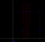
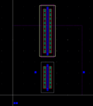
I've confronted a problem in Cadence layout design. I started with a simple inverter layout. The problem is, I cannot fit 2 transistors inside the selection box and cant stretch it either.
Can anyone help me with this? :bang::bang::bang::bang::bang::bang:
cadence.png

they should be inside that purple box !!
cadence.png

(I know I can use fingers or multipliers. I just want to know if there is another solution ... ?)
 

I assume that you created this layout in Layout XL using the Schematic-Driven Layout (Connectivity->Create) functionality. In that case, you should check whether the layer prBoundary is selectable or not.
 
it's not a problem :)

Just a right click on boundary, and make pr-boundary selectable. After that, you will be able to change the size of your boundary.
 
please right click on empty space in the PR boundary area (the blue rectangle).

after you will see an option:
Make PR Boundary Selectable,

please select and you will be able to control a blue lines.

IF it doesn't work>

go to the menu "Objects" by default it is in the layout window in the left-bottom corner (under layers menu). And add a mark to Select select-ability (S) for Boundaries.

Now you will be able to control your boundaries.

Enjoy
 
thank you.


I did something like this for the box.
Right click inside the box -> yes -> PR Boundary -> change width from 10 to 20

cadence.png

I also have another problem. After doing layout when I press create label nothing appears !!

it does not work at all !

cadence2.png

- - - Updated - - -

- - - Updated - - -

I think its related to software. Anyway thank you for help guys.
 

1) Check licensing and that File is Editable.
2) You could rotate both devices so they are parallel
3) Making one or both multifinger could make it fit.
4) prBoundary also needs to accommodate bussing,
half-spacings, access pin features and other
"overhead"
 
hello all,
I am working on cadence virtuoso using calibre tool for layout.In inverter while doing DRC,I am getting following errors which I am unable to solve since 1 month.

1) related to metal1,metal2,GC coverage. (metal1 coverage less than 0.3)
2) orthogonal corners are not allowed at die edge.
3) offgrid errors
4) sized AA density
5) metal area less than 0.414
 

For lone cells you should not be running whole-chip DRC
options such as pattern density and die-edge (die seal).
Also you may elect to ignore minimum metal area when
it pertains to the contacts, this will be fixed at the next
level up when you connect the cell to something. The
"off grid", that's you picking a bad setting for display
options (snap grid) inconsistent with the PDK rules. Get
with the program there, and move "whatever" to proper
grid (manually, or snap-to menu pick).
 

From where I can get the PDK rule? According to Design Rule, I am using snap spacing of 0.001 in 180nm technology
And what about the other errors besides offgrid?
 

Turn off the density check and die seal related DRC runset
options until you are working to finish the chip. Then most
of your errors will not be raised.

Read the DRC deck to determine what its grid expectation
is. 1nm seems kind of over-fine to me.
 
  • Like
Reactions: ADI21

    ADI21

    Points: 2
    Helpful Answer Positive Rating
How to turn off the density check and die seal?
I have also used snap spacing of 0.005,0.1,0.01. But still the errors are same.
 

You'd have to look in detail at the run options in the form
that kicks off the verification job. Somewhere in there
should be check-box options for subsets of the rules.

Snap spacing alone won't fix anything, snap spacing used
while editing is what forces things to be >= (or integer times)
grid. Maybe your problem is with old data, maybe not even
yours. The error report and highlighting ought to show you
specifically what and where; fixing it is then just another
layout activity.
 

Sorry but I couldn't understand what you said about run option.
When I select the offgrid error and coverage error, it highlights the whole layout. Only in orthogonal corner errors,it highlights the corners.So to remove that I modify the corners but in predefined modules(p-substrate and n-substrate),I am unable to do that.
 

How do you start the verification job? Isn't there a very
busy looking setup window that pops up, where you have
numerous options to check, fill and/or accept defaults?
 

No I have never seen this setup window which you are saying.
 

Well, then, you should show us how you do start a verification
job because it doesn't sound like how I've always done it in
Cadence, whether Diva or Assura or Caliber the menu driven
verification has always presented me a "control panel" window
first thing.
 

Hey thanks alot for the help but as I am just a beginner and don't have much knowledge about this verification job which you are saying. Can you please elaborate when this window pop up? Whether I have to click on some option in the menu or will it come up directly as I open the layout window?
 

I don't understand how you are doing this verification and
you don't understand anything I'm suggesting, so you need
to show us what you are doing. Take some screen shots as
you go through it, beginning from the layout view, step by
step, at least until you get to whatever is "run button".
 

Status
Not open for further replies.

Part and Inventory Search

Welcome to EDABoard.com

Sponsor

Back
Top