Continue to Site

Welcome to EDAboard.com

Welcome to our site! EDAboard.com is an international Electronics Discussion Forum focused on EDA software, circuits, schematics, books, theory, papers, asic, pld, 8051, DSP, Network, RF, Analog Design, PCB, Service Manuals... and a whole lot more! To participate you need to register. Registration is free. Click here to register now.

Help with 9-level SPWM MultiLevel Inverter

Status
Not open for further replies.

abhikuvar

Newbie level 6
Joined
Mar 5, 2014
Messages
14
Helped
1
Reputation
2
Reaction score
1
Trophy points
3
Activity points
118
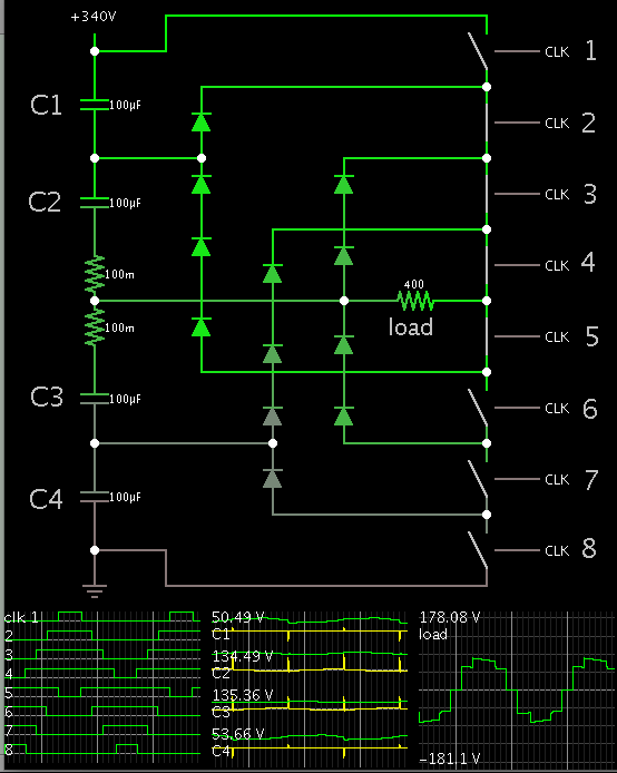
I am trying out a simulink model of 9-level multilevel inverter. I am using SPWM as modulation strategy for it. I am generating SPWM as follows as it is required by MLI

SPWMGen.JPG

And I am getting the gate signals as follows:

GatesSIG.JPG

Which I believe are the correct signals for 9-level SPWM Inverter to work properly. But when I apply those signals to the Cascaded H-bridge structure, I am getting just the 4 level weird output rather than 9-level output.

FYI, I am taking reference from 30V,60Hz rms sine wave and having 12V carriers for generating PWM because I am planning to build a prototype with above values.

Please let me know. Your comments are valuable and I appreciate helping me with this. I am attaching simulink model herewith. View attachment spwm_pulsegen.zip
 

It just so happens I have a simulation of a 5-level diode-clamped inverter. It illustrates the basic concepts of the sine-PWM type.


The scope traces show how the 8 clock signals behave. They create a blocky sine shape.

Does it looks different from your image of the gate signals?
 
I think, you have to have change the modulation method. I think you switch S1 and S2 of cell if associated PWM generates 1 ( cell generates Vdc at its output) and you have "NOT" this signal when associated PWM generates 0 (cell generated -Vdc at its output). this is what I guess. you can test by ordering PWM signals manually.
change the modulation method as when the reference is lower than saw tooth two upper switch or lower switch of the cell get on. (0 at cell output).
if problem would not solved send your simulation. meanwhile you can find simulation of a 15-level H-bridge ML online.

Good luck
 

Thanks for the simulation, BradTheRad. In my simulation I am using a 30Vrms, 60Hz sine wave as a modulating frequency and 10kHz triangular wave as carrier frequency. So my gate signals look typically high frequency at first and then they are at constant '1' for some time reverting back to high frequency part and so on.

In my post, the second waveform is plot of gate pulses itself. I think you are using more of a square shaped wave with constant frequency. I think that is what is different in here. Would you mind having a look at my Simulink file and see what is wrong with it? I mean I think I might be generating PWM signals in a wrong way.

- - - Updated - - -

Thanks, kappa_am.

Can you provide with the link to find 15-level H-bridge ML simulation?

I will try to brute force the PWM signals in my simulation and see what happens. I too believe there would be something wrong in providing gating pulses.

- - - Updated - - -

Hi kappa_am. Please find my simulation file here.
 

Attachments

  • spwm_pulsegen.zip
    22.1 KB · Views: 91

You have 8 gate signals. I believe the upper four should be reversed, so #4 is at the top.

The bottom four signals look fine. They resemble the bottom half of the sinewave.

Here is an article which gives diagrams of gating signals.

"A Single Phase Diode Clamped Multilevel Inverter and its Switching Function"
 
Thanks BradTheRad! I tried reversing the top 4 gate outputs. Surprisingly, the output looks the same, being just a 4-level weird output rather than a nine-level one. Please find image attached. I am not sure what is happening here.
pwm_output.JPG
 

I tried reversing the top 4 gate outputs. Surprisingly, the output looks the same, being just a 4-level weird output rather than a nine-level one.

That only has 4 signals. Originally you had 8. How did you lose half of them?

I thought your gate signals should look like this. (Your original image with the upper half inverted it in a graphics editor.)

9973273700_1411858686.jpg
 

    V

    Points: 2
    Helpful Answer Positive Rating
Thanks BradTheRad! I believe I did the same thing that you suggested. Let me show you in pictures what waveforms I am getting:

- So this is the output waveform of gating signals
gatingpulses.JPG

- the output voltage of all 4 cells combined
output.JPG

- individual voltages of the cells (there is a big problem here I do not why because of which this weird voltage is being output)
indiv_cells.JPG

- the whole arrangement.
arrangment.JPG

- - - Updated - - -

Please find attached this simulink file if you want to refer.

- - - Updated - - -

So, now I tried by giving the pulses manually. i.e. no high frequency stuff just some regular pulses which look like this:

pulsesnoHF.JPG

And the still the output which I am getting is like this,

output2.JPG

This looks like a similar problem and I don't understand why it is springing up!!
 

Attachments

  • spwm_pulsegen.rar
    24.4 KB · Views: 84

Your gating signals now appear correct.

It looks as though each capacitor (4 of them) is driven by an H-bridge.

Sorry, I'm not sufficiently familiar with this topology to point out where the problem is.

I also have no experience with Simulink.

Looking at your 'output' and 'output2' images... It looks as though the middle capacitors are not contributing to overall output. The voltage remains at low amplitude.

So, now I tried by giving the pulses manually. i.e. no high frequency stuff just some regular pulses which look like this:

I'm comparing this with my post #2. (I zoom in so your yellow scope trace is easy to see.)

Question: Shouldn't your gate pulses look similar to mine? (See 8 traces at bottom left). Notice how my upper 4 pulses overlap the bottom 4 pulses. Your upper and lower halves do not overlap at all. This explains the long dead times in your output2 image, whereas my output has only brief dead times.

Right now I am only referring to your regular simplified pulse diagram. I don't know if solving that will necessarily lead to success with your high-freq gate pulses.
 

when I saw your simulation I so believed that my guess is true!! your bridges out -vdc or vdc, just 2 level, while your bridges have to generate 3 level -vdc, vdc and 0. I mean you just turn off or turn on switches 1,2 or 3,4 while some times switches 1,3 or 2,4 must be turn on.

modify your modulation as below. when your reference is positive and higher than saw tooth turn on 1,2, as you have done. when reference is positive and lower than saw tooth turn on both upper switch 1,3. when your reference is negative and lower than saw tooth turn on 3,4. and when your reference is - and higher than saw tooth turn on two lower switch , 2,4. in this situation you can also switch on 13 but to use switches equally in practical circuits it better to do as I told.

good luck

- - - Updated - - -

P.S
i have attached an 11-level H-bridge. please study it and understand, because I don't like it be a reason of laziness. :)

Good Luck
 

Attachments

  • elevenlevelhbridge.rar
    29.9 KB · Views: 102

Status
Not open for further replies.

Part and Inventory Search

Welcome to EDABoard.com

Sponsor

Back
Top