Continue to Site

Welcome to EDAboard.com

Welcome to our site! EDAboard.com is an international Electronics Discussion Forum focused on EDA software, circuits, schematics, books, theory, papers, asic, pld, 8051, DSP, Network, RF, Analog Design, PCB, Service Manuals... and a whole lot more! To participate you need to register. Registration is free. Click here to register now.

Suggestions for filtering the Noise from the circuit output

Status
Not open for further replies.

patan.gova

Full Member level 3
Joined
Dec 19, 2011
Messages
172
Helped
4
Reputation
8
Reaction score
0
Trophy points
1,296
Activity points
2,776
Hello,
I am working with the Pulse(PPG) signal measurement.The circuit implemented is shown here**broken link removed** but the reference for this is taken form https://embedded-lab.com/blog/?p=5508 Some of the components in the circuit are replaced namely Phototransistor with NRJC5501RView attachment 8508.NJL5501R_E_20130418.pdf) and OPAMP with TIA OPA381(https://www.ti.com/lit/gpn/opa380), and gain here used is 1+Rf/Ri=1+680K/1.2K=567.The output of the implemented circuit is shown here

Noise_signal.png

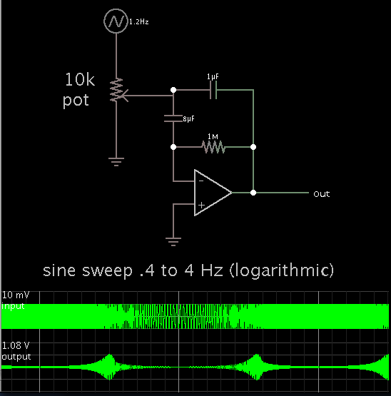
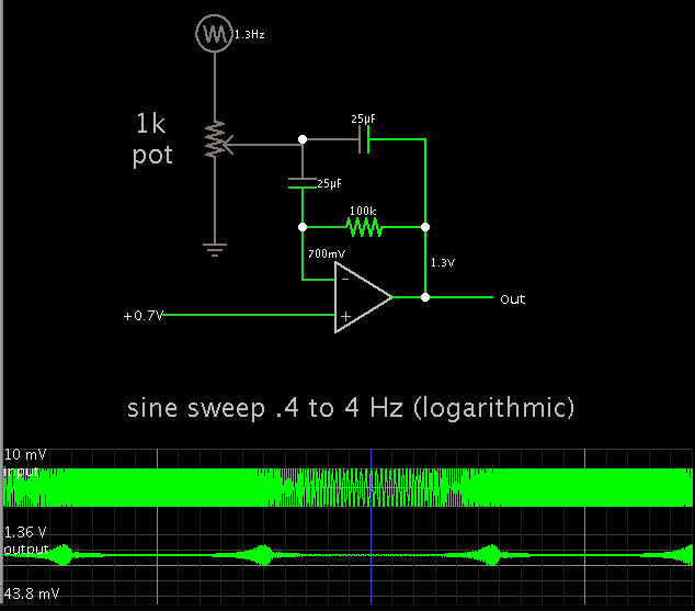
The filters are designed to allow the frequency components in the range of 0.7 to 2.3Hz as the required PPG signals are in this range.
The output seems to be nearly okay but the Noise(frequency components) indicated with the red portion is annoying.I am not sure why this is coming.
Can someone suggest changes in the circuit or if any other sort of filters are to be used so that noise can be removed resulting in a clear pulse signal which is finally needed.
Thanks in Advance.
 
Last edited:

Can someone suggest a idea to filter the noise?
 

The signal doesn't look like being effectively low-pass filtered. The low-pass in the first link apparently can't be considered as effective filter.

By the way, did you verify that the noise is actually picked-up by the photodiode?
 

Hello FvM,
Yes,I verified it as the actual (direct) output signal of the photo diode was not showing any Pulse type signal but after passing through filtering stage the output was pulse signal as shown in the post[1] but with noise.
Is there any better way to design the filter for band pass filters in the range of 0.7 to 2.3Hz.
 

I see.

OPA381 isn't a regular OP and not designed to work in a circuit like this. It's probably oscillating.
 

The circuit in this thread uses a photo-diode that is strangely FORWARD-BIASED. Most photo-diodes are either reverse-biased or have no bias voltage.
The circuit shows a normal opamp in a non-inverting circuit but the OPA381 is a transimpedance amplifier, not an opamp and it is always used in an inverting circuit.

The OPA381 in this thread has no power supply connected to it.
 

Can someone suggest changes in the circuit or if any other sort of filters are to be used so that noise can be removed resulting in a clear pulse signal which is finally needed.

The link below has designs for narrow bandpass and wide bandpass filters (see about halfway down the webpage).

I can't say for certain that it will be noise-free in your application.

https://www.ti.com/lit/an/sloa093/sloa093.pdf

- - - Updated - - -

This is a simulation that seems to suit your frequency range.


@Audioguru:1.The circuit shows a normal opamp in a non-inverting circuit but the OPA381 is a transimpedance amplifier, not an opamp and it is always used in an inverting circuit.
> So, should I change the OPA381 input to inverting in the circuit.
2.The OPA381 in this thread has no power supply connected to it.
>Sorry, I havn't shown power supply connections in the circuit but pin7(V+) was supplied with +3V and pin4(V-) was grounded as described in the datasheet attached below.

@BradtheRad: Thanks for sharing good information material.
And for the simulated circuit above can you explain a bit about this
1)Is this a kind of narrow band pass filter with single supply (as I am not able to match this with the filters in the link you provided)
2)Will this act as a band pass filter for 0.4 to 4Hz while amplifying the signal.
Thanks.
 

Attachments

  • opa381.pdf
    487 KB · Views: 98

@Audioguru:Yes, I will feed the input of photodiode to the inverting terminal of OPA381 but I am wondering of

1)which circuit is to be implemented to get 0.7 to 2.3Hz bandpass filter characteristics as in the attached datasheet of OPA381 as there are different possible ways of implementation like in 8,9,10,11 pages.Which one should I choose and how to adjust it so that it only passes only a partuclar range of frequencies.

2)Or should I pick a widebandpass filter design implementation as in the link posted by BradtheRad https://www.ti.com/lit/an/sloa093/sloa093.pdf

3)what about the simulated circuit posted by BradtheRad.Is this the widebandpass filter ? How to calculations can be made to arrive at 0.4 to 4Hz.

Can someone explain the above so that a circuit with OPA381 can be implemented that passes the band of frequencies in the range of around 0.6 to 2.5 while amplifying the signal.
Thanks in Advance.
 
Last edited:

@BradtheRad: Thanks for sharing good information material.
And for the simulated circuit above can you explain a bit about this
1)Is this a kind of narrow band pass filter with single supply (as I am not able to match this with the filters in the link you provided)
2)Will this act as a band pass filter for 0.4 to 4Hz while amplifying the signal.
Thanks.

I started with the narrow BP type (Fig. 11 in the TI article). It is a conceptual schematic, and you will need to experiment to find the best way to adapt it to your sensor.

I adjusted capacitor values to produce a center frequency of 1.3 Hz. (3 uF worked.)

Then I redrew it so I could replace two resistors with a potentiometer. This permits you to alter gain to suit your needs (and to some degree the input impedance).

The resulting bandwidth appeared much narrower than your specified range of 0.7 to 2.3 Hz. So I played with component values. In particular I created a mismatch between the two capacitor values. It did not increase the bandwidth much.

I have revised the schematic.

By applying a positive voltage to the non-inverting input, the circuit now works with a single supply. (Fig. 12.) I made the two capacitor values identical, as the calculations indicate.

If you wish for the output to occupy the positive region, then the output capacitor is unnecessary.

I omitted an input capacitor since I'm not sure your photodiode will produce usable waveforms when it is in series with a capacitor.


Furthermore I reduced the potentiometer value and the feedback resistor value. This changed the center frequency, which required that I use higher capacitor values.

Because, looking closely at your scope image...

The noise spikes are evenly spaced. This includes the spikes on your ascending and descending waveforms. I believe the noise is mains hum. It is common to pick up mains hum in an input loop which is unshielded or lengthy or has high impedance.

I think your noise problem will be reduced if you can reduce impedances in your photodiode/input components, and if you use a shielded input lead.
 
The datasheet for the OPA381 transimpedance amplifier shows DC-coupled and very wideband signals. It can be followed by a low frequency bandpass filter.

Tube type or fluorescent lights produce mains hum spikes like that.
The rows of contacts and the tangled wires on a breadboard pick up mains hum interference spikes like that.
 

Hello,
@BradtheRad: I implemented the simulated circuit you suggested on the board.I built the same except the 20uF instead of the 25uF. And varied the input resistance(potentiometer) from 500 to 3k.
Otuput: When the finger is placed first time on the photo transistor the output signal voltage was high and then slowly decreased and after a while it was not giving any pulse.It is showing similar response when the finger is removed and placed for first .The constant keeping of finger is not resulting in any pulse or signal as shown in the result image.

**broken link removed**

Is there anything you can suggest about this circuit.
Thanks.

@Audioguru
The datasheet for the OPA381 transimpedance amplifier shows DC-coupled and very wideband signals. It can be followed by a low frequency bandpass filter.

I looked the datasheet to implement the Tran simpedance Amplifier as a first stage and then low frequency bandpass filter but I was confused with somethings in the datasheet as listed below
1)The capacitance and resistance of the phototransistor has not mentioned in the datasheet Can I assume them as 'Zero'.As they are needed for calculating Bandwidht(f at -3db) as described in the page10 of OPA381 datasheet and calculating noise zero, 'fZ' in page11.

2)What is the difference between 'fz' and 'f @ -3db'.If a range of frequencies I am interested is 0.5 or 0.7 to 2.4Hz how will they account for this.How they can be calculated if the next has to be frequency filtering stage.

3)Should I use the figure 6(b) or 6(c) circuit for the implementation as 6(c) has additional filter for further reducing the Output noise.How to select between them as the output will given to the second stage of low frequency bandpass filter.

Can someone explain a bit clearly about the above things.

As my main requirement is to amplify the small photo transistor signal using trans impedance amplifier and to allow the output signal frequencies in the range 0.5/0.7 to 2.3Hz.

Thanks in Advance.
 
Last edited:

I looked the datasheet to implement the Tran simpedance Amplifier as a first stage and then low frequency bandpass filter but I was confused with somethings in the datasheet as listed below
1)The capacitance and resistance of the phototransistor has not mentioned in the datasheet Can I assume them as 'Zero'.As they are needed for calculating Bandwidht(f at -3db) as described in the page10 of OPA381 datasheet and calculating noise zero, 'fZ' in page11.
The datasheet shows a very sensitive circuit where leakage resistance of the photodiode reduces it. Your sensitivity will be fine.
The datasheet shows a very wide bandwidth circuit where the capacitance of the photodiode reduces it. Your bandwidth requirement is very low.
Make certain that you have reversed the polarity of tour photodiode so it is as shown in the datasheet.

2)What is the difference between 'fz' and 'f @ -3db'.If a range of frequencies I am interested is 0.5 or 0.7 to 2.4Hz how will they account for this.How they can be calculated if the next has to be frequency filtering stage.
The transimpedance amplifier works well up to 3MHz but high frequencies do not matter in your circuit. The filter sets your very low bandwidth.

3)Should I use the figure 6(b) or 6(c) circuit for the implementation as 6(c) has additional filter for further reducing the Output noise.How to select between them as the output will given to the second stage of low frequency bandpass filter.
Figure 6(c) cuts high frequencies twice as well as figure 6(b). Most noise is at high frequencies that you do not have.

As my main requirement is to amplify the small photo transistor signal using trans impedance amplifier and to allow the output signal frequencies in the range 0.5/0.7 to 2.3Hz.
Did you replace the photodiode with a photo-transistor? Then the circuit will be different.
 

@Audioguru: I haven't used the phototransistor with TIA but I will.And how the circuit will be differ between the two(with photodiode and phototransistor).Do I need to modify anything in the figure6(c) circuit to work with photo-transistor.
Thanks.
 

Hello,
@BradtheRad: I implemented the simulated circuit you suggested on the board.I built the same except the 20uF instead of the 25uF. And varied the input resistance(potentiometer) from 500 to 3k.
Otuput: When the finger is placed first time on the photo transistor the output signal voltage was high and then slowly decreased and after a while it was not giving any pulse.It is showing similar response when the finger is removed and placed for first .The constant keeping of finger is not resulting in any pulse or signal as shown in the result image.

**broken link removed**

Is there anything you can suggest about this circuit.
Thanks.

Sorry, your attachment brought up an error message.

What you describe is typically what happens when a capacitor is in series with DC pulses (presumably coming from your sensor diode).

Each DC pulse charges the capacitor a little more. Eventually it is charged to a point that it no longer passes the signal.

If this is happening with your bandpass filter, then you must modify your circuit so as to feed it true AC.
 

Implemented phototransistor with Transimpedance Amplifier as shown in the figure6(C) of OPA381 datasheet gives the following:
The components used are same as in the datasheet figure6(C) except the photodiode is replaced by Phototransistor as shown in this image **broken link removed**

And the output signal is here with
1)50mv/div **broken link removed**
2)200mv/div **broken link removed**

Can someone explain about the things listed below
1)Will the signal be improved if the bandwidth is limited to 3Hz(as requirement lies between 0.5 to 2.4Hz) and increasing the gain by Rf or it should be directly given to the filtering stage.
2)As it is mentioned in datasheet page11 like "all required gain should occur in the transimpedance stage, since adding gain after the transimpedance amplifier generally produces poorer noise performance".how the gain can be increased.
3)Also the signal is having a DC value which is making the signal to be located at around 780mV because of the bias voltage I guess.How to make the signal to located at 0V.
4)which filter should be used for the next step the narrow bandpass filter or widebandpass filter from here(https://www.ti.com/lit/an/sloa093/sloa093.pdf) or a different type of filter is needed.
5)In the datasheet(page11) 'fz' is mentioned.How it will account for the circuit output's and should it be considered for the circuit design.
Suggestions are needed if anything else is needed to make it a better pulse signal.
 
Last edited:

You are mixing up things.
A reverse-biased or no-bias photodiode uses an inverting transimpedance amplifier.
A photo-transistor uses a non-inverting opamp amplifier.
 
@Audioguru:As mentioned earlier the phototransistor implementaion with the circuit here of first stage implementation resulted this
**broken link removed** and **broken link removed**

As said before it is showing mains hum now also.How to overcome this mains hum.What is your suggestion like is there any other type of circuit of implementing this phototransistor with transimpedance amplifier.
As you mentioned earlier in this post https://www.edaboard.com/threads/301340/ about using opamp voltage follower with a gain of 1 and feeding its output to the sallenkey lowpass filter.Can I know what will be the difference in using in 1)https://embedded-lab.com/blog/?p=5508 only the first stage 2) as your mentioned opamp voltage follower with a gain of 1 followed by asallen-key lowpass filter.anywasy both will be using phototransistor in non-inverting mode.

I hope that I can choose the one of the best.
Thanks in Advance.
 
Last edited:

The first schematic you posted shows a photodiode (not a photo-transistor). The photodiode is connected backwards. It drives a non-inverting opamp (not an inverting transimpedance amplifier).
The second schematic shows a photo-transistor driving a non-inverting opamp.

In your first post you said you replaced the photo-transistor with a different one and WRONGLY replaced the non-inverting opamp with an inverting transimpedance amplifier. In your other posts you said you used a photodiode.

In my post (#12) I said that the mains hum might be from fluorescent lights or interference from messy wires all over the place on a breadboard.

The circuit from Embedded Lab DOES NOT have a Sallen-Key lowpass filter, it has an extremely simple RC filter so its opamp can have a very high gain and does not need to be driven from the low impedance of an opamp like a Sallen-Key filter must be.
 

Status
Not open for further replies.

Part and Inventory Search

Welcome to EDABoard.com

Sponsor

Back
Top