Continue to Site

Welcome to EDAboard.com

Welcome to our site! EDAboard.com is an international Electronics Discussion Forum focused on EDA software, circuits, schematics, books, theory, papers, asic, pld, 8051, DSP, Network, RF, Analog Design, PCB, Service Manuals... and a whole lot more! To participate you need to register. Registration is free. Click here to register now.

2stage fully differential opamp output distortion

Status
Not open for further replies.

tompham

Full Member level 2
Joined
May 29, 2010
Messages
133
Helped
29
Reputation
60
Reaction score
29
Trophy points
1,308
Location
usa
Activity points
2,066
Hi all

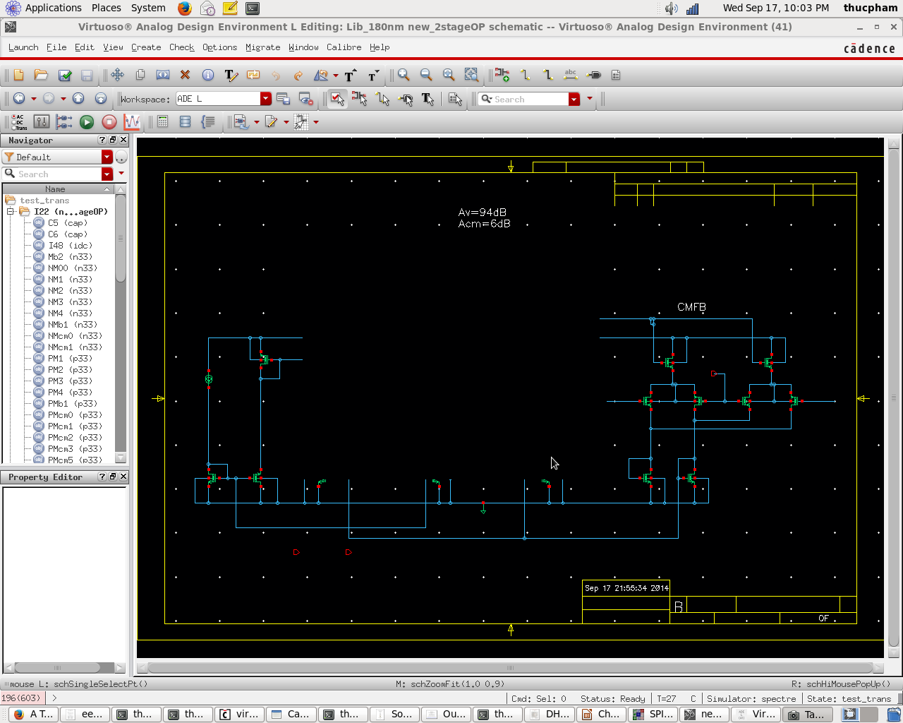
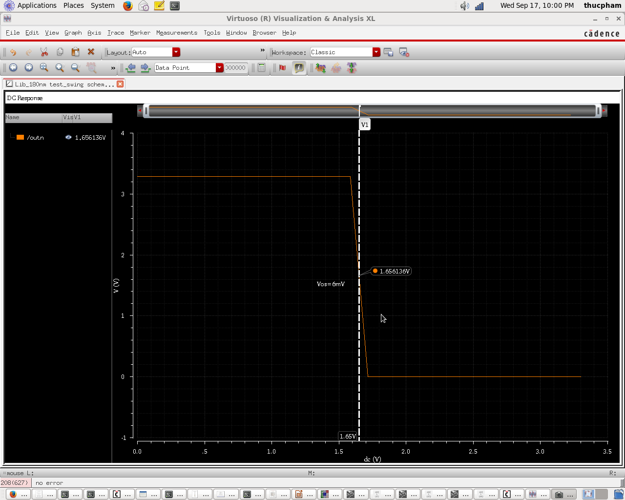
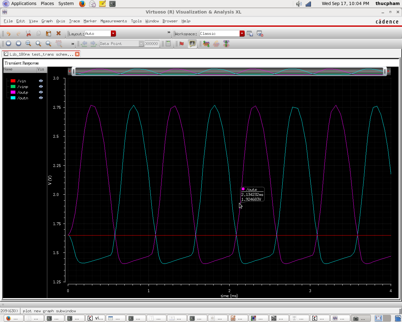
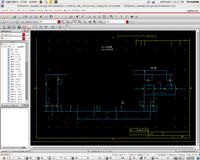
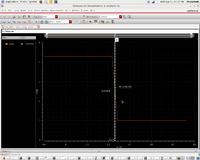
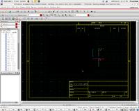
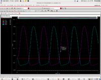
Im desinging 2 stage fully differential opamp with continous cmfb. My design using smic18mmrf with VDD=3.3v and input cm = output cm = 1.65v. I test transient with apply sin wave 20uV peak to peak
to see how output behave. From the waveform (see attached) , the output distortion at below output common mode. I have hard time to figure the problem even the opamp has good output swing. Anyone can help me with this. Thanks a lot


You see in picture 4 what the actual output swing is (either if it's considered good or not). Shouldn't the CM bias be centered to the output voltage range?

The other question is why the output clips below 1.5 V. I fear , this can't be seen from your selected circuit snippets.
 

Hi FvM

Thanks for your response. I use common mode reference = 1.65v = vdd/2
This is clip below 1.5v from my simulation
 

It's look like your current sink controlled by CMFB has very poor performance. Add some degeneration to them or cascodes and check what will happen.
 

The clipping at 1.5V reminds me of typical op amp behavior.
Example, LM741, whose output cannot go closer than a couple volts above its bottom supply rail.
 

The clipping at 1.5V reminds me of typical op amp behavior.
Example, LM741, whose output cannot go closer than a couple volts above its bottom supply rail.

Yeah, but not for cmos process with 3.3V supply ;-). I gues that diff pair is loaded by simple current source maded on one nmos so the lower rail limitation is equal to VDSsat voltage around 0.2-0.3V.
 

Status
Not open for further replies.

Similar threads

Part and Inventory Search

Welcome to EDABoard.com

Sponsor

Back
Top