Continue to Site

Welcome to EDAboard.com

Welcome to our site! EDAboard.com is an international Electronics Discussion Forum focused on EDA software, circuits, schematics, books, theory, papers, asic, pld, 8051, DSP, Network, RF, Analog Design, PCB, Service Manuals... and a whole lot more! To participate you need to register. Registration is free. Click here to register now.

2 Layer Board Routing Guidelines

Status
Not open for further replies.

BabaYaga

Advanced Member level 4
Joined
Aug 1, 2012
Messages
106
Helped
10
Reputation
20
Reaction score
10
Trophy points
1,298
Location
Hyderabad
Activity points
1,295
Hi Guys,
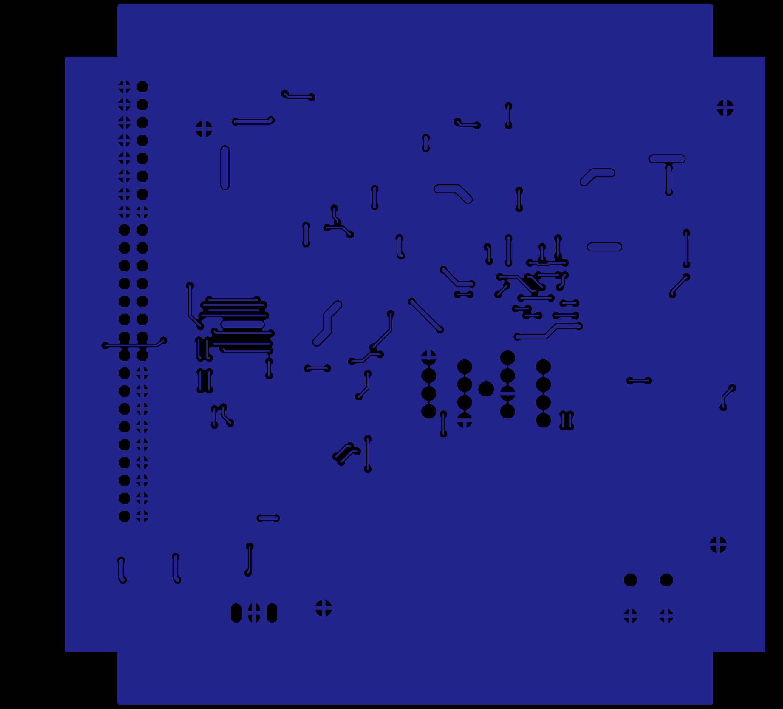
I have done High Speed Multi-Layer PCB Design, but never did any 2 Layer system Design, Now i need to design a 2 layer PCB for a PIC Microcontroller with some ADCs and DACs, so my queries are:
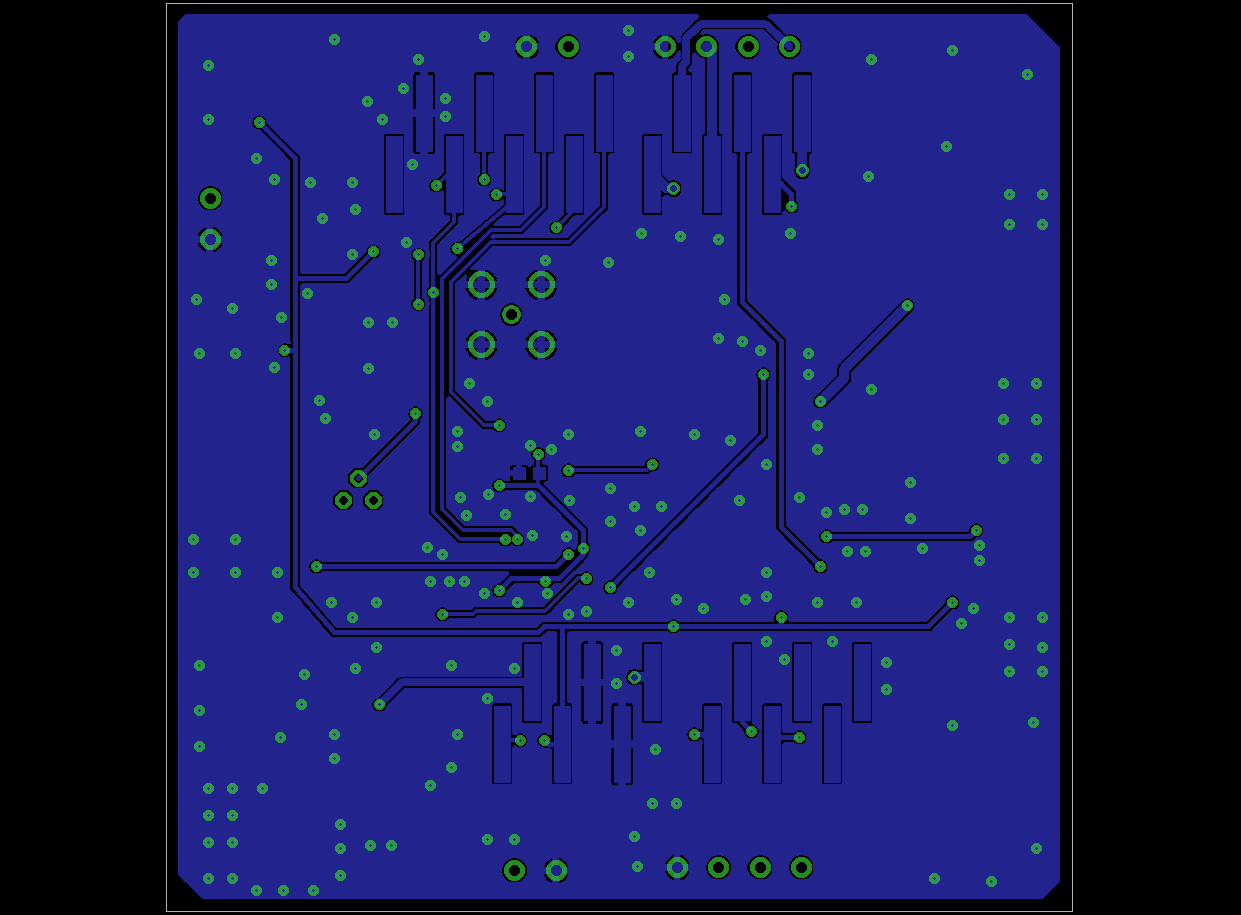
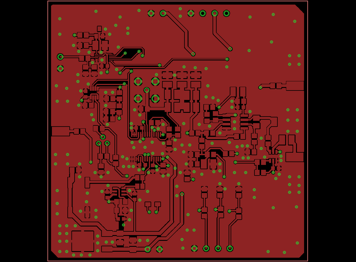
1 - I have seen some 2 layer Pcbs with copper pouring for GND, please explain this?
2 - Can i directly route signals as i wish without being concerned about the return paths etc.,(Basically what measures i need to take in connecting signals)?
3 - How do i handle Power?(Do i need to build planes or can i connect directly through thick traces)
These are some of my queries, feel free in suggesting anything relevant to the above topics.

Regards
BhavaniT
 

Hello BhanvaniT,

I have seen some 2 layer Pcbs with copper pouring for GND, please explain this?
Sometimes one layer will be use as electric shielding in high frequency circuits. the layer is connected to GND.

Can i directly route signals as i wish without being concerned about the return paths etc.,(Basically what measures i need to take in connecting signals)?
Yes, you can. Only take care that you not get a capacitive feedback from input to output.

How do i handle Power?(Do i need to build planes or can i connect directly through thick traces)
You can use the power connection as normal signal lines, like you want. take only care for decoupling capacitors, but I think you know this for multilayer. It's the same, I hope. I only use single layer for my designs. :smile:

Regards

Rainer
 
Thanks rfredel for the reply,


"Sometimes one layer will be use as electric shielding in high frequency circuits. the layer is connected to GND."

1 - what if both sides of the Pcb are filled with copper? (i have seen recently such a 2 layer Pcb)

"Yes, you can. Only take care that you not get a capacitive feedback from input to output."

2 - What do u mean by capacitive feedback, how is it caused and how do i prevent it?

3 - Which one is the most effective one for power routing, Thick Trace or Plane and why?

Regards
 

Hello,

what if both sides of the Pcb are filled with copper? (i have seen recently such a 2 layer Pcb)
It's the same, like I write before. Electric shielding. Sometimes a layout program has a function called "Automatic Ground-Plane" to automaticly fill empty place with copper as GND. This is usefull in high frequency circuits to protect agains unwanted effects.

What do u mean by capacitive feedback, how is it caused and how do i prevent it?
Capacitiv feedback can happen, if input and output signallines are to close together for a long way. Sensitive for this are digital-, audio- and high frequency circuits.

Which one is the most effective one for power routing, Thick Trace or Plane and why?
The thickness of the traces is dependent of the current and the thickness of copperfoil.
Here you can look for some details.

Regards

Rainer
 
You're still dealing with the same laws of physics, so things like return current paths still matter if you have high frequency signals. This is problematic for 2 layer designs since you often need to have signals and components on both sides, meaning that some signals will not have continuous reference planes and return paths. In that case, methods like stitching capacitors can be helpful, but not always.
 
A good 2 layer board is more difficult that a 4 layer. You have no ground plane between the top & bottom layers to minimise cross coupling of signals so you need to be constantly aware of what tracks you are routing over/under. Avoid running track directly over tracks on the other side - make any overlap short. Assuming you use surface mount and put the components on the top, any tracks on the bottom remove parts of your ground plane so you need to minimise use of the bottom layer for tracking. EMC can be an issue without a good ground plane.

None of that matters if there is nothing critical on the board - clocks, high impedance signals, low level signals etc, but usually you have all of those things.

Keith
 
If the design needs 4+ layers then it needs 4+ layers and you should use 4+ layers and tell the managers they are clueless.

If the design can easily be done on 2 layers then you will have to be more careful about your placement, keep your components placed so that there is as little track cross over between layers as possible.

Route power and ground in thick tracks around the board first, try to keep them all on the bottom side so that signals can go on the top, then you can put copper flooding wherever you can get it connected to ground, if you have room on the top side then it may also be good to put copper flooding stitched to the bottom side so that you balance out the copper weight on both sides to prevent warping.

Most other principles are the same, keep tracks short, put pin to pin rtc.

You will have to make allowances for not having more layers, compromise on some design rules and decide which rules is more important to follow.


If you have not done 2 layer boards before then I guess that you started out the easy way :) :)
 
Two layer board with PICs ADCs DACs is going to be a compromise, you need to optimise placement so that the opposite side of the board is as near a contigous ground plane as possible.
Download this for current:
https://www.saturnpcb.com/pcb_toolkit.htm
in my view using 2 layers these days is silly, with the requirements for signalintegrity, even the most basic digital device having silly rise times and the EMC requirements (CE FCC)it can cost more to do a 2 layer board instead of doing the job properly and using at least 4 layers. It is taking cost cutting to the extreme, and have never seen a proper justification for the minimal cost saved these days. Though I have seen numerous cut down designs(2 layers) that have CE marks on them but do not pass testing.
Ultimatley you need to know the rise times of signals on your board, clock frequencies and convertor resoltion, using these facts help determine the design complxity.
 
The purpose of the design hasn't been said. If it's intended to comply with regulations for active and passive EMC, I agree with marce.

Recent single chip processors have moderate active EMC behaviour, e.g. low level crystal oscillators with soft clock edges, but a 2 layer design may still fail in ESD and RF succeptibility if it has some wires connected to the outer world.

If the board population allows for an almost continuous ground plane, there's a chance to get off with 2 layer.
 
TIP, use zero ohm resistors to jump tracks if you do have to use 2 layers, minimisimg bottom layer traces so helps get a better ground plane.
Quite often 2 layer designs will work, and work quite well if the requirements are pretty mundane, but with DACs and ADCs you can loose convertor resolution down at the bottom (least significant) bits due to the extra noise over a multilayer design.
 
Professional PCB designers suggest that return path should be at least 1 Di-electric apart... avoid Loops and 90 degree turns in routing .... place digital components aside from Analog... use coupling cap. and ground sheilding
 
Er we are proffessional PCB designers.
The return plane would have to be at least one dielectric apart, otherwise things would get a bit hot:)
You have described things in very simple terms, each of the items you mention have multiple papers and information behing them explaining in detail what and why they affect the signal and the overall performance of the board.
The attached text file provides some links to explain these concepts, expect a lot of bed time reading.:grin:
 

Attachments

  • PCB related links.txt
    5 KB · Views: 106
As has been said, minimise the use of the ground plane layers, even using jumpers. This is the bottom of a 2 layer surface mount PCB (no jumpers).


Keith
 
In my lab we etch our own 2 layer boards whenever possible (sure is nice to design and build a board in the same day), and I often get around the EMC issues by employing lots of ground vias and stitch capacitors. Here's a layout for a 180MHz DDS shield for an Arduino:


The bottom ground plane isn't continuous at all, but it's routed such that the return paths of all high frequency signals are uninterrupted, so it still works out. I doubt it would win any awards for EMC compliance, but it did work quite well for prototyping purposes.
 

Thank You rfredel.

- - - Updated - - -

@mtwieg,
I have heard of stitching vias but not about stitching capacitor, what is it?, can you please explain a little.

- - - Updated - - -

Thank you @keith1200rs,
I got your point, but its really difficult sometimes to realize whether our circuit is critical enough or not and do we need some critical designing strategies or not, especially in a 2 layer board. I'm actually using PIC16LF877A - 4MHz clock, MAX11205, MAX5216. looking at the datasheets of this data converters they seem to be not so severe in terms of layout, but still i'm wary.

- - - Updated - - -

@cyberrat,
when i started the board it was supposed to be a simple PIC16LF877A board for evaluation purposes then later on the PCB real estate was so intriguing that i went on adding stuff and complicated life, now i want to execute this board on a 2 layer since i never did any 2 layer, mutilayer FPGA systems was my thing, but now i want to make some microcontroller boards with 2 layer pcbs. Thanks for the suggestions.

- - - Updated - - -

@marce,
Thank you so much for the program you have provided, I was in desperate need of such a program just to make sure that my layout practices are precise enough.
i will start using it from now on, considering you are well versed with this tool, i hope i can disturb you if i have any tool related queries.

Thank you once again for the tool.

- - - Updated - - -

@FvM,
I have given a solid ground plane on the bottom layer, and layout is almost done, i will post the pictures of the layout, as soon as i complete it, as far as application is concerned i'm using a PIC16LF877A microcontroller with MAX11205 and MAX5216.

- - - Updated - - -

@marce,
once again thanks for those links, they are really awesome in terms of content, Thanks a lot.

- - - Updated - - -

As i said, my layout is complete, and these are the images of the top and bottom layers, somehow they seem very crude to me, but its my first 2 layer board so please excuse all my mistakes but let me know what are those mistakes.

TOP.JPGBottom.JPG


Thank you for all the intel guys, it was really a great learning experience.
 

You can never be sure how good a 2 layer board is going to be - it is usually down to practice and experience. Your componentry doesn't sound too demanding.

I try to avoid chopping the ground plane up too much by trying to keep tracks all on one layer, even if that means taking a track from the bottom to the top and back to the bottom, even when it could simply have stayed on the bottom. It may not make any difference, but provided you aren't doing it with a critical signal, it doesn't do any harm either. You have a few tracks on the ground layer that fall into that category.

The other thing is to try to avoid gaps in the ground. You have a couple of places where close tracking on the ground has meant there is not enough room for the ground between them. If you move a track or two the ground can run between them.

Overall it doesn't look like you would have problems. My PCB was for a tester and had an AD8302 on it and worked fine.

Keith.
 
@keith1200rs.

Unfortunately i have some signals on the bottom plane, and that's the best possible way that i am able to do it, that's because, if i move those signals and try to increase some spacing, then it is falling right below some of the signals on the top layer and i feel this is much more riskier than it is right now, and moreover this is the optimum trace length that i can get.

Thank You
 

Status
Not open for further replies.

Part and Inventory Search

Welcome to EDABoard.com

Sponsor

Back
Top