Continue to Site

Welcome to EDAboard.com

Welcome to our site! EDAboard.com is an international Electronics Discussion Forum focused on EDA software, circuits, schematics, books, theory, papers, asic, pld, 8051, DSP, Network, RF, Analog Design, PCB, Service Manuals... and a whole lot more! To participate you need to register. Registration is free. Click here to register now.

General Components to be used in hardware for pic18f452

Status
Not open for further replies.

huzeeigat

Member level 4
Joined
Mar 18, 2012
Messages
75
Helped
3
Reputation
6
Reaction score
2
Trophy points
1,288
Location
Andheri
Activity points
1,776
Hello everyone..
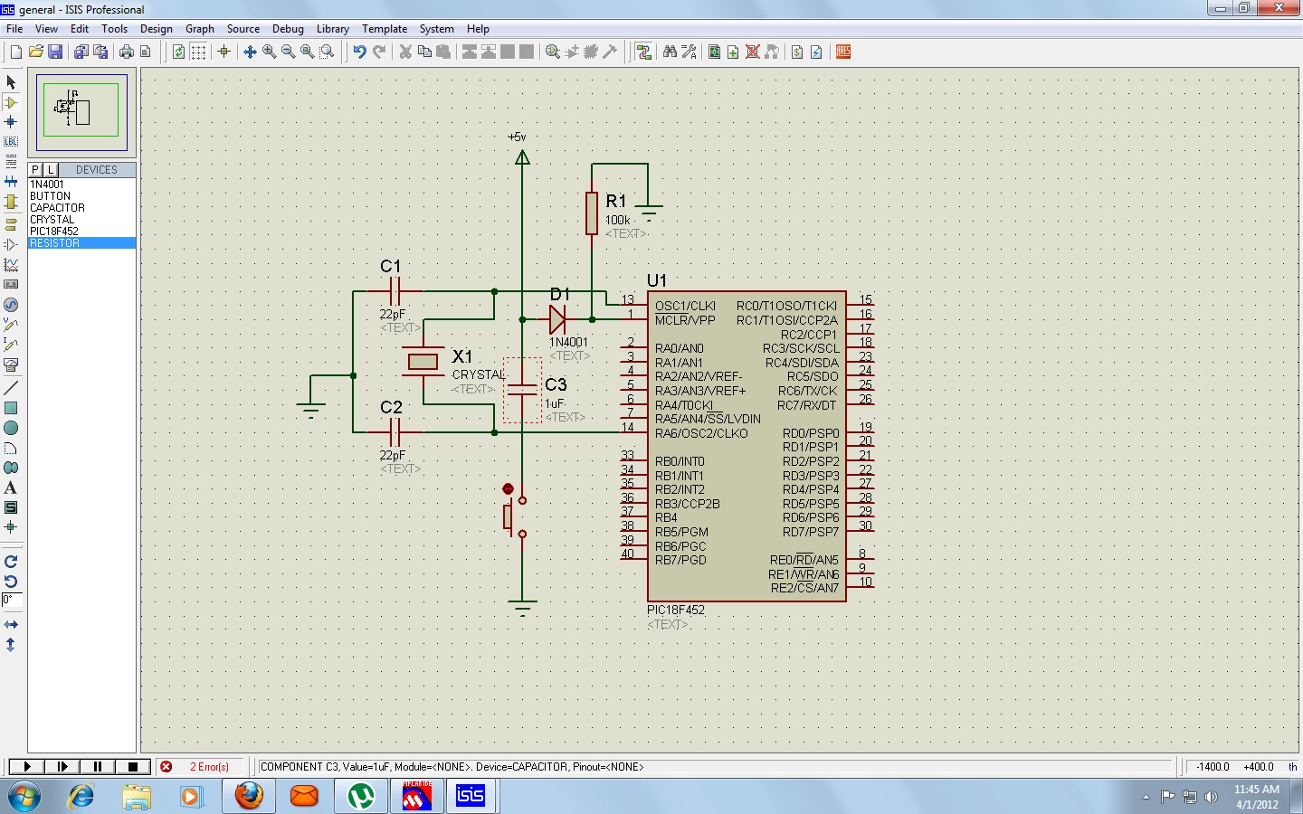
I am making a project using pic18f452..i just want to know which are the components generally used in hardware with pic18f452..so that i dont get an error while implementing it in hardware..
I am uploading a image of what i know is generally necessary...

---------- Post added at 19:40 ---------- Previous post was at 19:38 ----------


---------- Post added at 19:41 ---------- Previous post was at 19:40 ----------

Also i want to know whether the capacitors used are electrolytic or ceramic?

---------- Post added at 19:41 ---------- Previous post was at 19:41 ----------

In the above image the crystal is of 10mhz..

---------- Post added at 20:43 ---------- Previous post was at 19:41 ----------

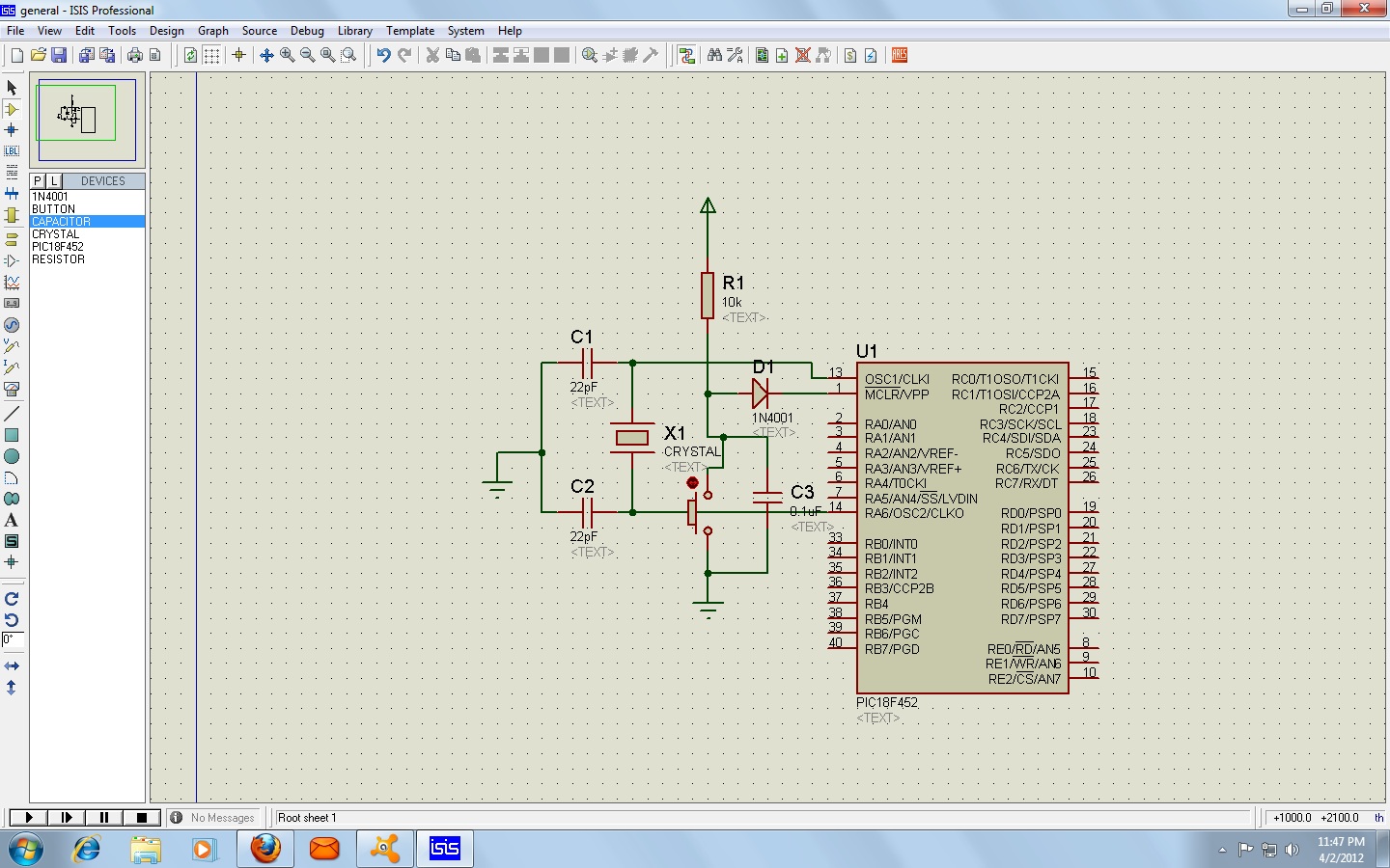
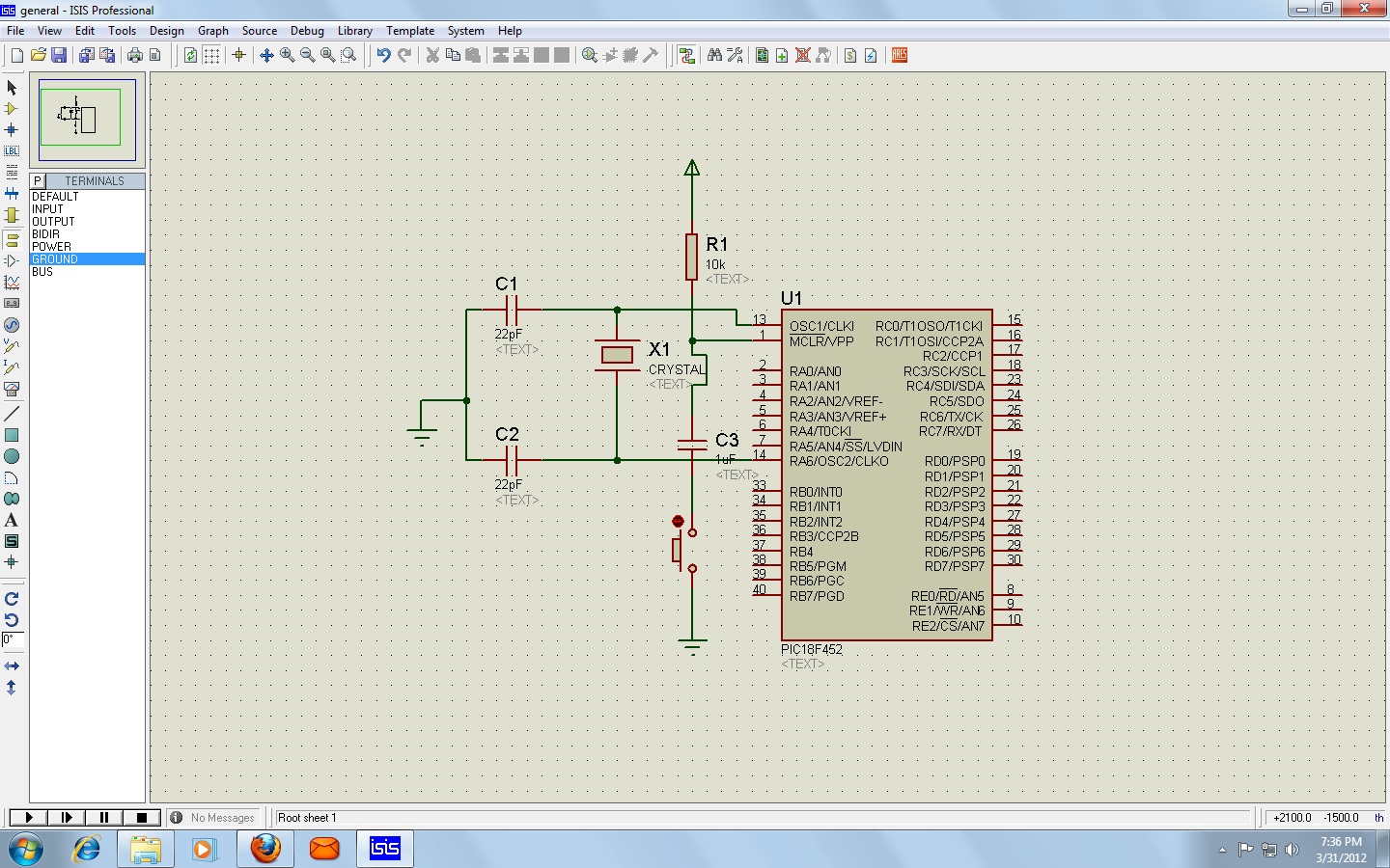
I wanted to know whether i require external pull up resistances for any of i/o ports..and do i have to connect pins 11,12,31,32 to vcc and ground respectively as mentioned in data sheet...
 

and do i have to connect pins 11,12,31,32 to vcc and ground respectively as mentioned in data sheet...

11, 12 and 32, 31 to VDD and ground(VSS). 11 and 32 to VDD, 12 and 31 to ground(VSS).

Also i want to know whether the capacitors used are electrolytic or ceramic?
C1 and C2 in your diagram will be ceramic capacitors.

Across the VDD and ground lines, connect 0.1uF ceramic capacitors and a 10uF electrolytic capacitor.

I wanted to know whether i require external pull up resistances for any of i/o ports..
If you decide to use RA4 (PORTA 4 - pin 6) as output, it's open drain. Then, you need to connect a pull-up resistor. Otherwise, pull-up resistor is not needed when the port pins are to be used as outputs. When they are to be inputs, it depends on that specific situation.

Also, make sure to take care of the ADC and comparator modules in code when using the associated pins.

Hope this helps.
Tahmid.
 
11, 12 and 32, 31 to VDD and ground(VSS). 11 and 32 to VDD, 12 and 31 to ground(VSS).


C1 and C2 in your diagram will be ceramic capacitors.

Across the VDD and ground lines, connect 0.1uF ceramic capacitors and a 10uF electrolytic capacitor.


If you decide to use RA4 (PORTA 4 - pin 6) as output, it's open drain. Then, you need to connect a pull-up resistor. Otherwise, pull-up resistor is not needed when the port pins are to be used as outputs. When they are to be inputs, it depends on that specific situation.

Also, make sure to take care of the ADC and comparator modules in code when using the associated pins.

Hope this helps.
Tahmid.

Thanks tahmid..I didnt get you how do i connect 0.1uF ceramic and 10uF electrolytic capacitor..
And in which cases do i need to connect pull up resistor if i use the port pins as i/ps...
 

Connect a 0.1uF ceramic capacitor across pins 11 and 12, another across pins 31 and 32. Connect a 10uF electrolytic capacitor between the +5V and ground (take care of the polarity).

If you use port pins as inputs, it will depend on the type of input which will dictate if you need to use a pull-up or not.
If you have an input that is either 0 or 1, you don't need a pull-up.
If you have an input that is 1 or floating, you need to connect a pull-down.
If you have an input that is 0 or floating, you need to connect a pull-up.

You can't allow the input to be floating.

Hope this helps.
Tahmid.
 
@Tahmid: Thank you very much...
The range for a digital 0 is:- 0-0.5v and for 1 is:- 3.3-5v..am i correct?
and what should be the value of pull up and pull down resistance if i need to connect one..?
 

One last thing- your reset RC won't work more than once. There is no path to discharge the C (unless of course you are in an Iranian atomic bomb facility where the stray radiation will discharge it, haha). Tie the bottom side of C3 to ground and put the reset switch across both sides of C3. If you are using an ICD (in-circuit-debugger) your reset circuit will keep the debugger from working. If you are using the ICD, remove *everything* (including the reset switch) on the reset circuit and only put a 100K ohm resistor to ground on the MCLR pin (the reset can be controlled by the ICD) .

Good luck. You'll have fun with the 18F452.
 

@Tahmid: What is your opinion about this...??
And also is Capacitor C3 is electrolytic or ceramic?
 

Look in the lower right corner of the following Microchip document under "Target Circuit Design Considerations": "No capacitors on MCLR"
https://ww1.microchip.com/downloads/en/DeviceDoc/51265g.pdf

My mistake on the 100k. It should be to VCC. When you have an RC reset circuit and an ICD connection, the common point of the RC network goes to the anode of a diode. The cathode of the diode goes to a 100K R and to the MCLR pin. The other side of the resistor goes to ground.
 
Last edited:

Almost - take D1 cathode and top of C3 to Vcc through a 4.7k resistor. Take bottom side of C3 to ground. Put reset switch across C3.
 

But if i connect d1 cathode to vcc through 4.7k to vcc..the same point will be at ground..i dnt understand what u are exactly trying to say....


Here's a schematic of a PIC I did a couple of years ago.
 

Here's a little clearer view of the schematic (pic2.doc)
 

Attachments

  • pic2.doc
    106.5 KB · Views: 51

the file i downloaded is corrupted.. am unable to see from image
 

Here's a portable-document-format of a drawing-exchange-format embedded in a Microsoft Word document. What has the world come to?
 

Attachments

  • pic2.pdf
    23.4 KB · Views: 48

I would suggest using PIC18f4520 instead. It is an upgraded PIC18f with compatible pinouts as PIC18f452. You can use the user manual present in download section of **broken link removed** as a reference for your schematic.
 

@Tahmid: Thank you very much...
The range for a digital 0 is:- 0-0.5v and for 1 is:- 3.3-5v..am i correct?
and what should be the value of pull up and pull down resistance if i need to connect one..?

For pull-up or pull-down, you can use 10kΩ resistor. You can't expect to draw much current through the resistor anyways.

For C3, use a 0.1µF ceramic capacitor.

And as mentioned, use C3 across the switch so that closing the switch discharges C3.

Hope this helps.
Tahmid.
 
@Tahmid: Thanks...so the circuit in image i uploaded is correct just need to connect a 0.1uf cap across c3..and tell me..if i am using the adc and the i/p to the pins is in the range of 0-0.5v always do i need a pull up..and also what do you mean by floating i/p?
 

If you have an analogue input, then you don't need to connect a pull-up or pull-down. On the contrary, the pull-up or pull-down may "mess" the analogue value depending on the input impedance. So, don't connect a pull-up or pull-down unless it's a low impedance input (like from the output of an analogue buffer/voltage follower).

Do you use in-circuit serial programming?

I assume you're referring to the image in post #9.

Remove C3 and connect the switch between pin 1 (MCLR) and ground. Connect C3 across the switch. Between D1 anode and +5V, connect a 10k resistor. Or you could connect D1 anode to +5V and connect the 10k resistor between the cathode and pin 1 (MCLR).

Remove R1.

Hope this helps.
Tahmid.


---------- Post added at 23:49 ---------- Previous post was at 23:48 ----------

is this what u were trying to say?
 

Status
Not open for further replies.

Similar threads

Part and Inventory Search

Welcome to EDABoard.com

Sponsor

Back
Top