Continue to Site

Welcome to EDAboard.com

Welcome to our site! EDAboard.com is an international Electronics Discussion Forum focused on EDA software, circuits, schematics, books, theory, papers, asic, pld, 8051, DSP, Network, RF, Analog Design, PCB, Service Manuals... and a whole lot more! To participate you need to register. Registration is free. Click here to register now.

Issue with 4046 PLL Phase Comparator 2

Status
Not open for further replies.

lnm

Newbie level 4
Joined
Mar 17, 2011
Messages
7
Helped
1
Reputation
2
Reaction score
1
Trophy points
1,283
Location
Madison, WI
Activity points
1,372
I'm new to the forum, so I hope this post is in the right place.

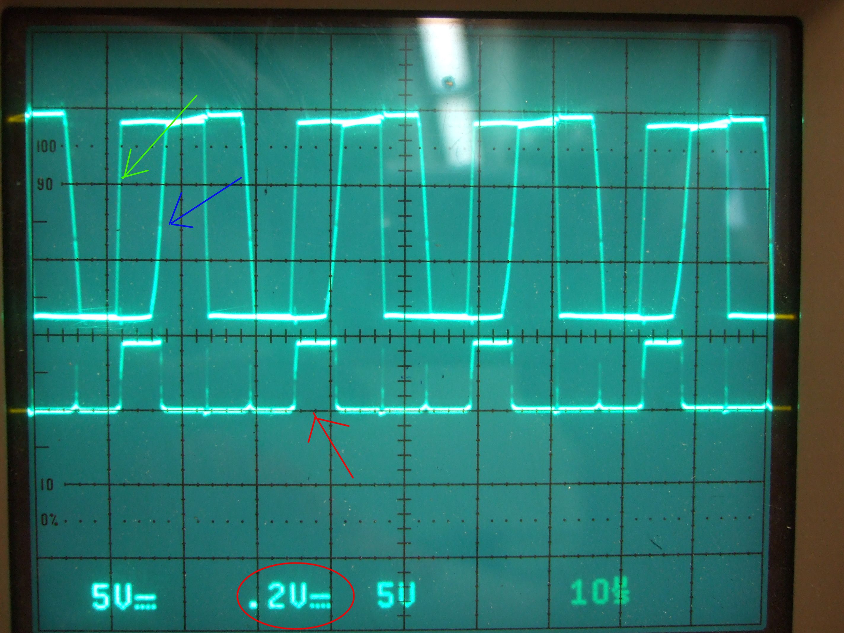
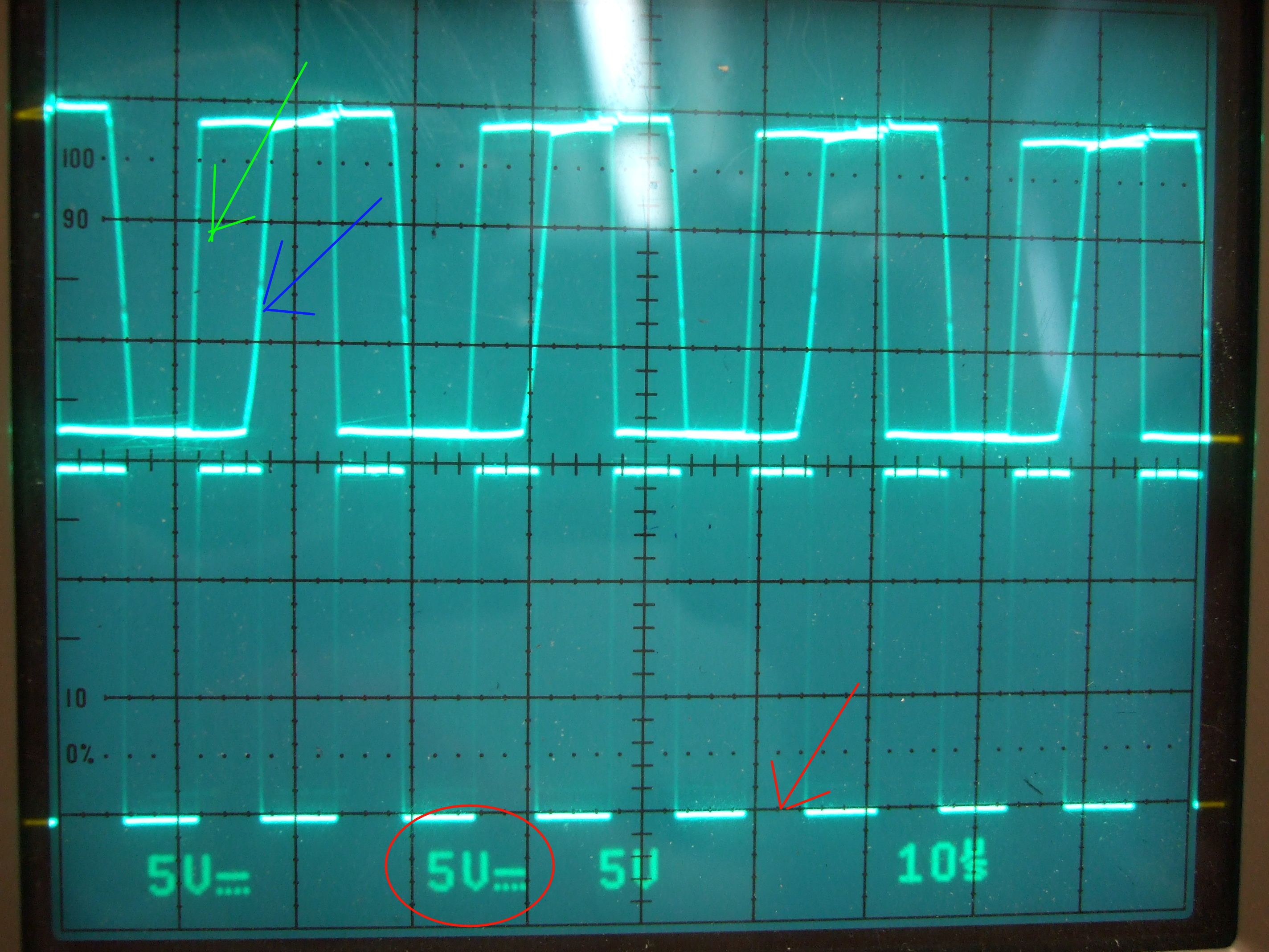
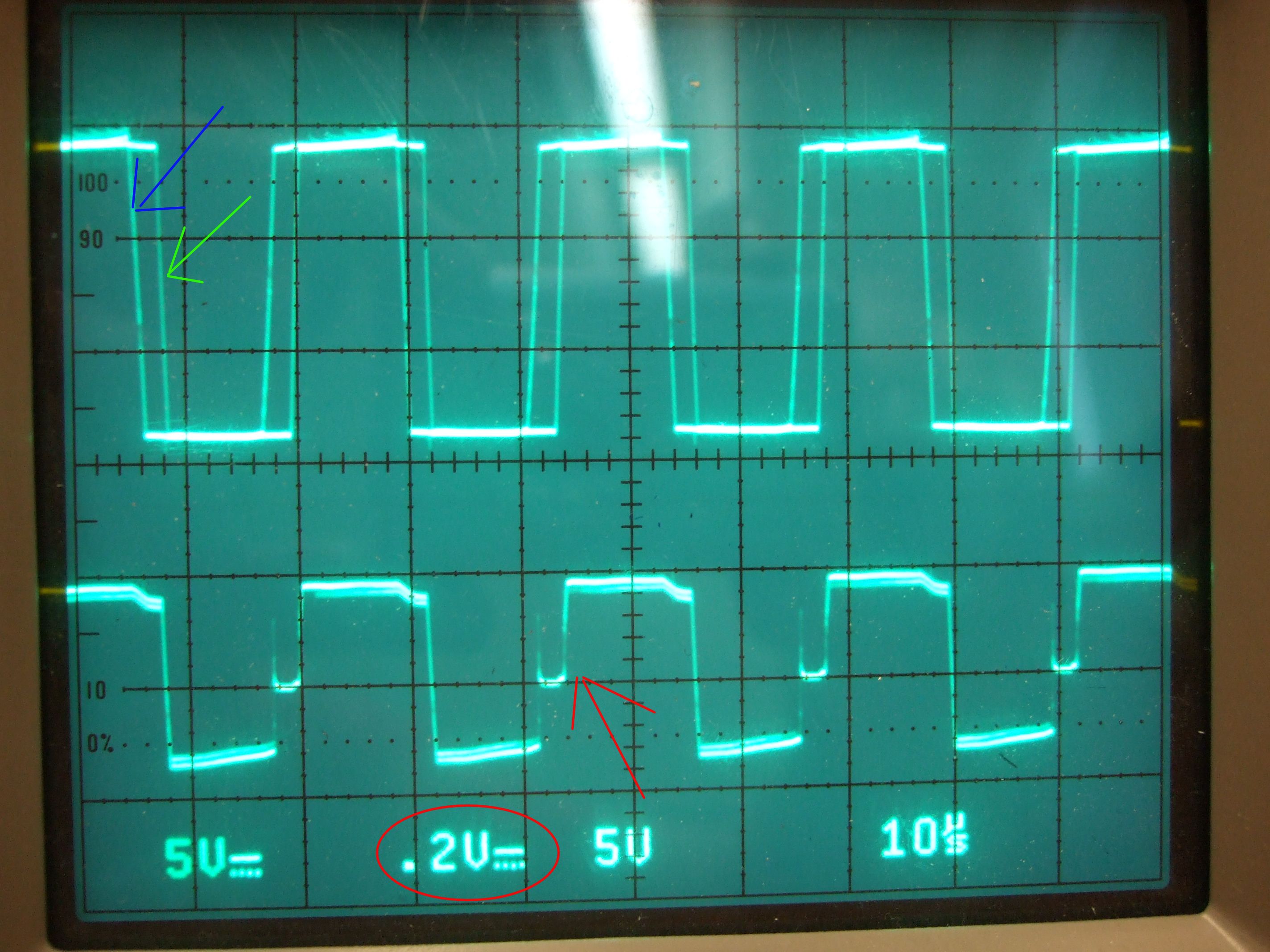
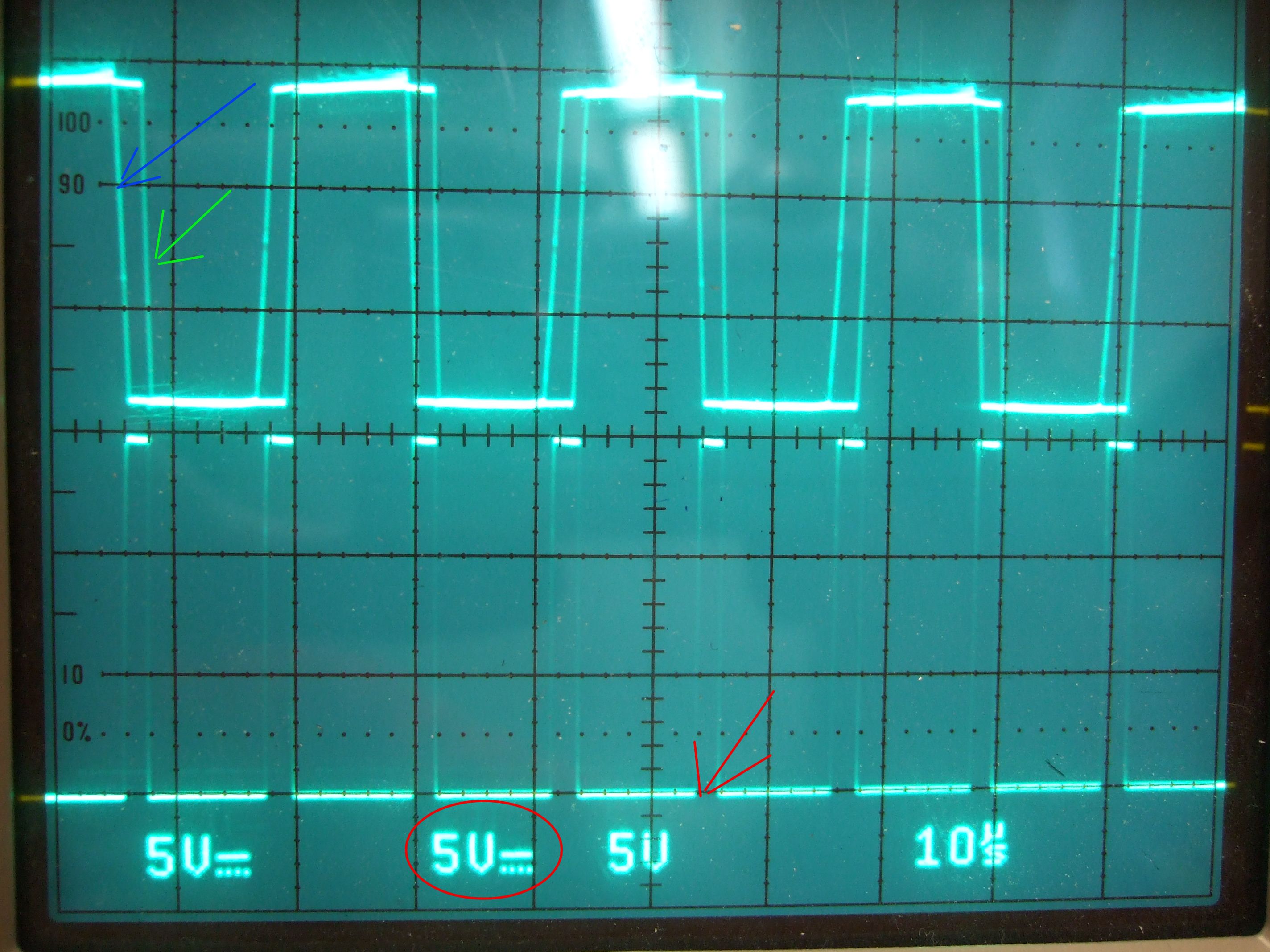
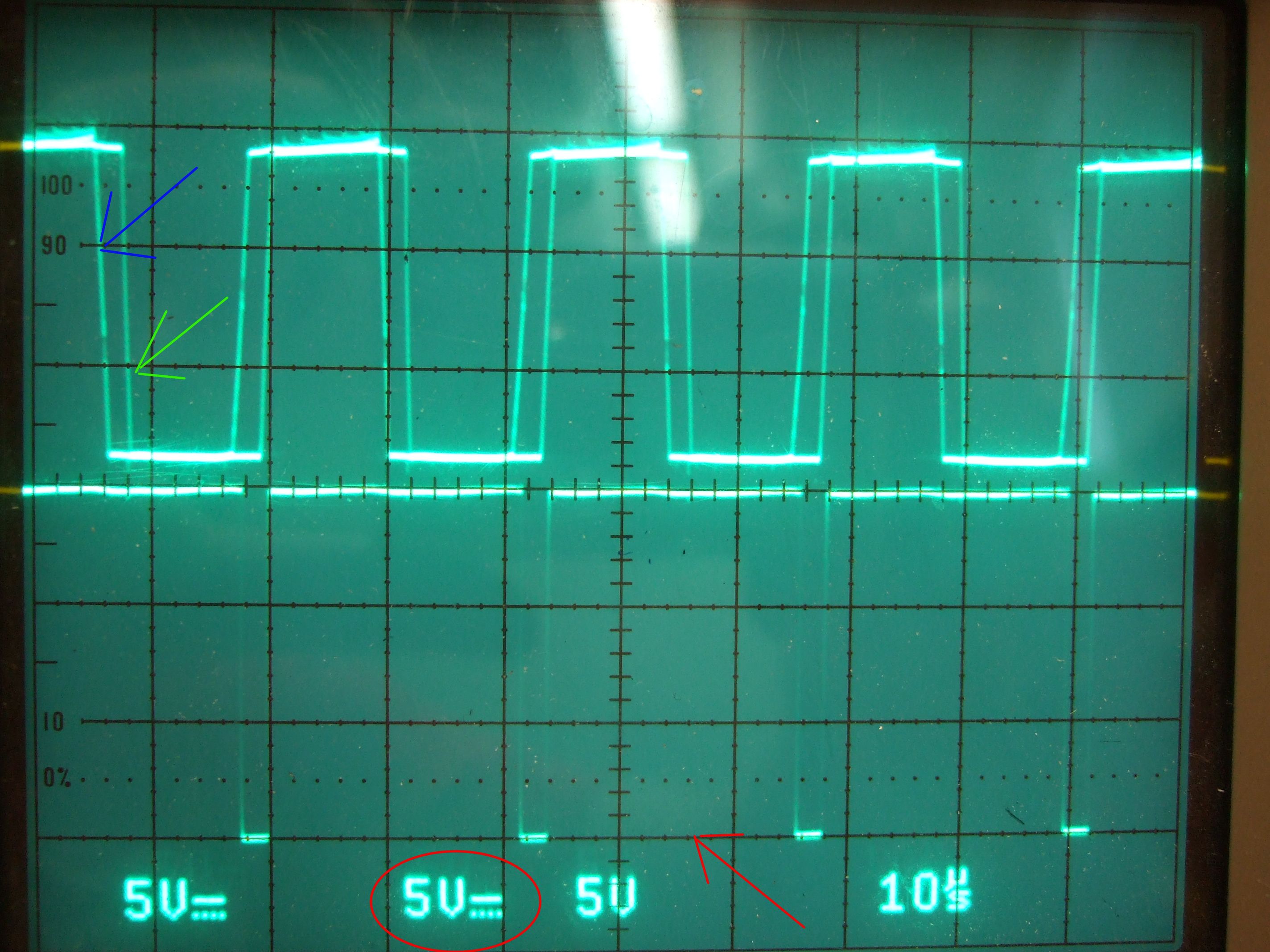
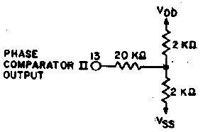
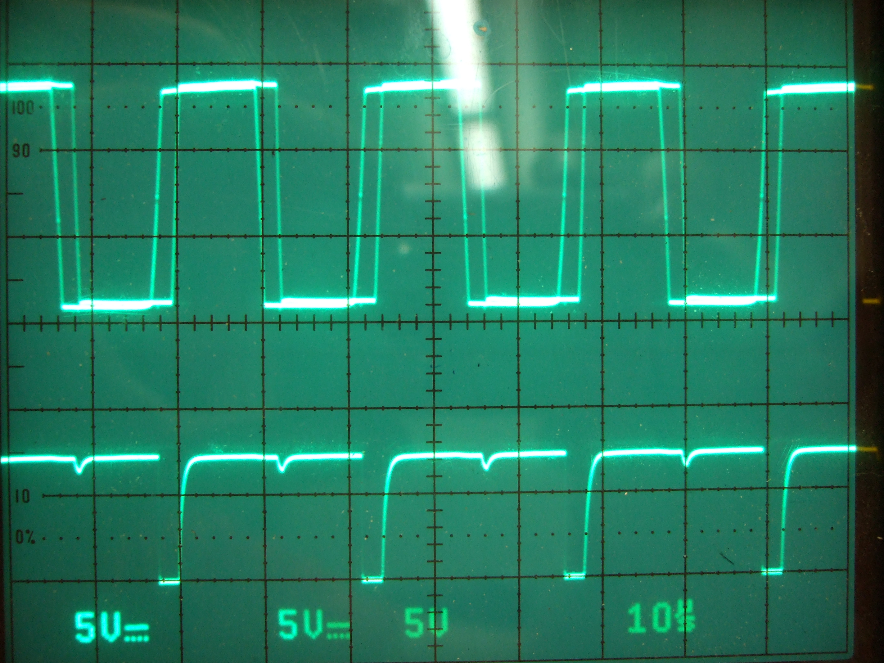
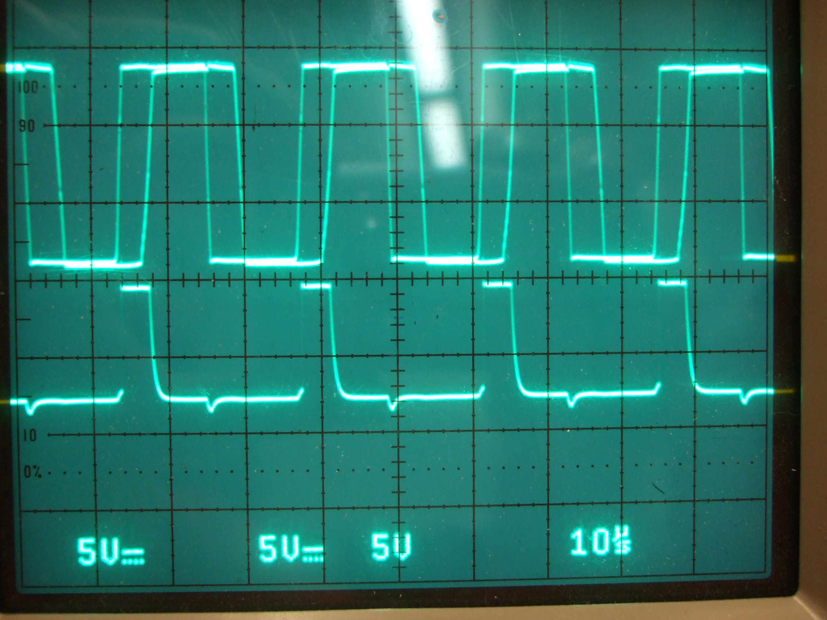
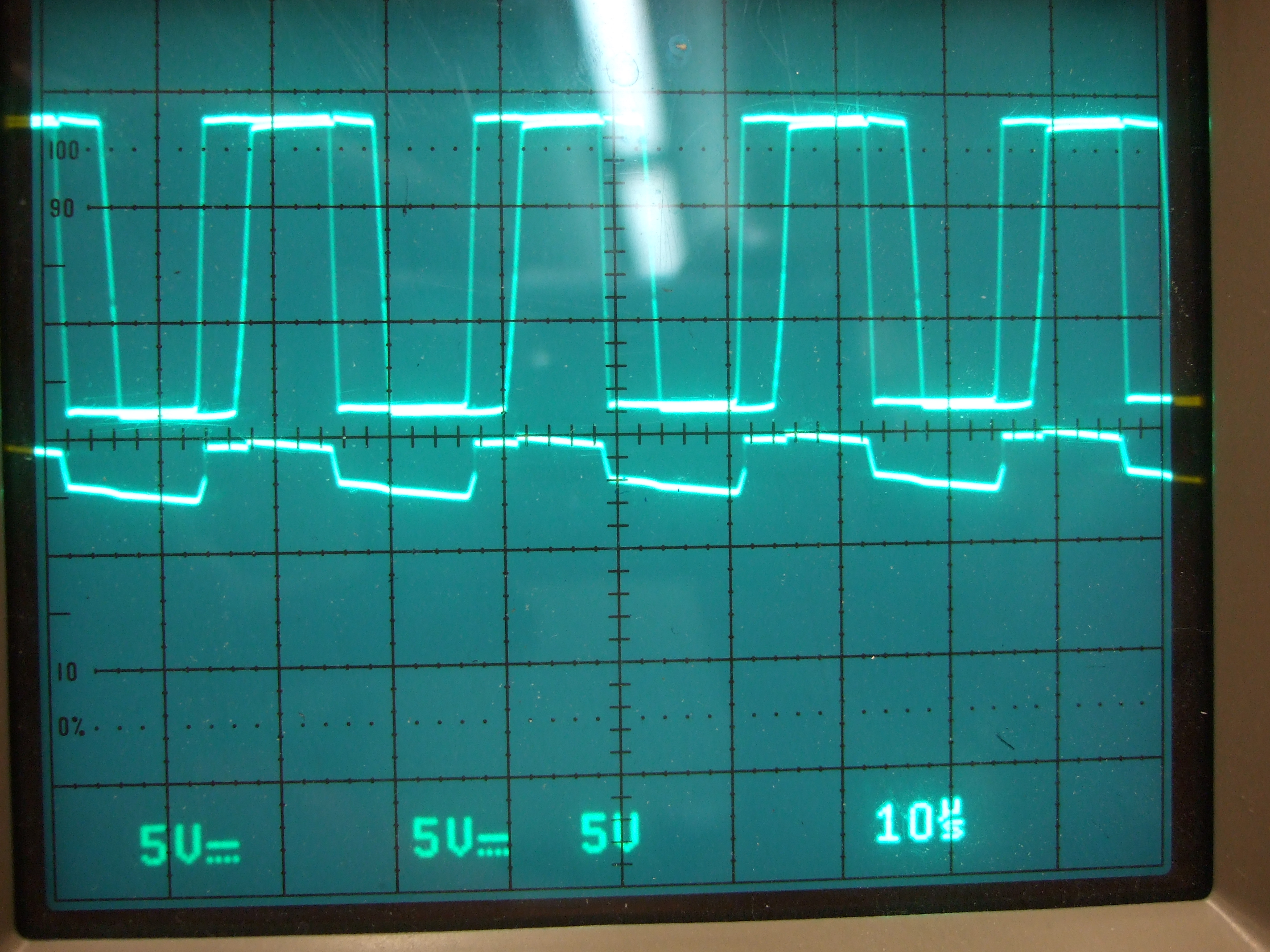
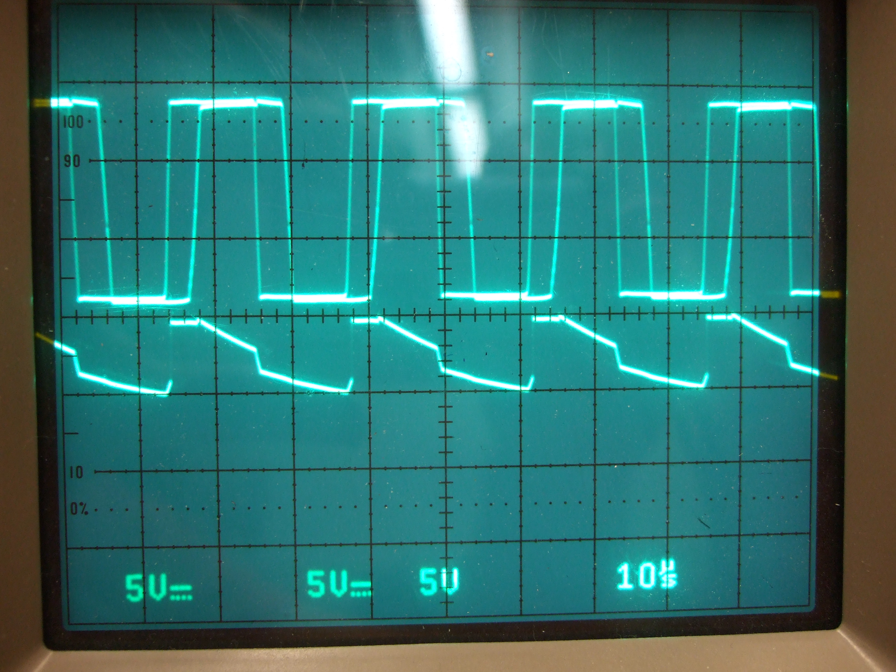
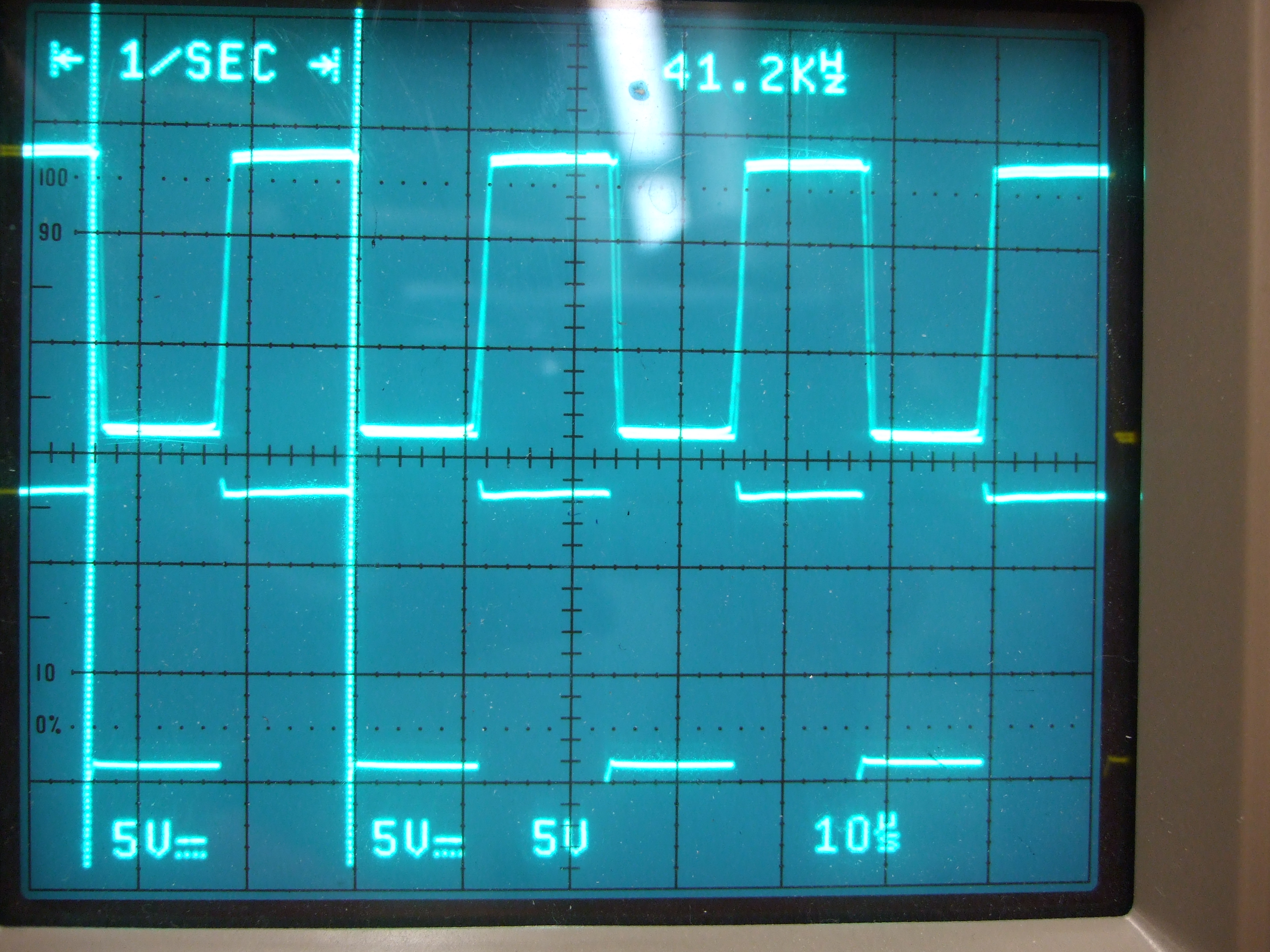
I'm trying to use the 4046's phase comparator 2, but the output isn't doing what I'd expect. Based on the **broken link removed**, I expect the output to be Vdd, Vss, or high impedance, but I'm only seeing very small output voltages even without any load attached to it (e.g. when it should be Vdd -- 15V in my circuit -- it's only a fraction of a volt). Everything else in the chip (VCO, phase comparator 1's output, etc.) seems to work fine, so I figured it was just a bad chip, but I just tried several different chips from two different manufactures and they all behave the same way.

Both of the input signals to the phase comparators are square waves that are something like 1.5V when low and 13.5V when high, so I don't think they'd be causing trouble (plus, phase comparator 1 doesn't have a problem with them). However, figure 3.4 on this German site seems to indicate I shouldn't have a rail to rail square wave input, although neither my German not google translate's English is good enough to tell me why (although it sounds like it's only an occasional problem).

Am I misinterpreting the datasheet? Is there some trick to making that output do its thing?

If there are no obvious tricks I should know, I can try capturing and sharing some oscilloscope traces to show what I'm talking about.
 

Using two signal generators at the input (pin 3 and 14), varying the frequency of one generators you should see pulses at the comparator output (pin 13), and also when the signals at the input are in phase should see pulses output at pin 1. Activity on pin 1 means your PLL is locked.
In the same time just for information can take a look to the output of comparator nr 1 at pin 2 (comp. nr 1 and comp. 2 have the same inputs)
 

I'll try putting in different frequency signals to test the device, but I'm ultimately interested in comparing the phases of two signals at the same frequency but different phases (after converting the square wave of the VCO to a sine wave, I'll be driving a resonator, so on resonance it'll have no reactance and the phase difference will be zero). Here's what the **broken link removed** says about comparing signals of the same frequency:

When the p-type or n-type drivers are ON, they pull the output up to VDD or down to VSS respectively.

...

If the signal input and comparator input frequencies are equal, but the signal input lags the comparator input in phase, the n-type output driver is maintained ON for a time corresponding to the phase difference. If the comparator input lags the signal input in phase, the p-type output driver is maintained ON for a time corresponding to the phase difference. Subsequently, the voltage at the capacitor of the low-pass filter connected to this phase comparator is adjusted until the signal and comparator inputs are equal in both phase and frequency. At this stable point, both p and n-type drivers remain OFF and thus the phase comparator output becomes an open circuit and keeps the voltage at the capacitor of the low-pass filter constant.

Below are links to some oscilloscope traces. The top two traces are the inputs shown at 5V per division. The green arrow points out what the datasheet calls the “comparator input”, and the blue arrow points out what the datasheet calls the “signal input”. The trace in the bottom half of the screen is the output. Its scale is shown in the red ellipse and the ground value for the trace is pointed out by the red arrow.

Signal input lags comparator input, looking at PC2out:


The n-type outputs should be on, pulling us to VSS, and we're getting a small signal, so I guess that's ok.

Signal input lags comparator input, looking at PC1out:


The output looks fine on phase comparator 1; it's 0V when they're the same and 15V when they're different.

Comparator input lags signal input, looking at PC2out:


The p-type outputs should be on, so we should be seeing VDD (15V), but instead it only goes up to about 0.2V and we see this wacky signal which even goes down to about -0.1V! This is the case where something seems to be obviously wrong.

Comparator input lags signal input, looking at PC1out:


Again, it looks fine.

Comparator input lags signal input, looking at PCPout:

The phase comparator pulse output is connected to phase comparator 2. I'm not sure exactly what it's output should look like, but its output does correspond to the phase difference.


Any thoughts on what's going on?
 
Last edited:

The "wacky" signal that you see at PC2 output is normal. Those intermediate steps are normal (as can be seen also in the datasheet).
What is not ok is the negative -0.1V that you get, but this could be just a measurement error (seems you are using an old analog scope).
All other waveforms looks fine for me.
Just build a small PLL using a simple VCO and see how the circuit behaves when is phase locked.
 

That signal goes from -0.1V to 0.2V. Is that really normal? Shouldn't it go up to 15V?

I'm not ready to dismiss that negative voltage so quickly. It doesn't show up anywhere else and that scope may be old, but it shouldn't have a 0.1V offset (indeed, I've never seen it have a 0.1V offset before).
 
Last edited:

Yes, the amplitude at PC2 is too low, when the waveform seems to be fine.
Could be a bad component at the PC2 output which can put the signal to the ground, otherwise I cannot see what the problem is.
 

In 4046 phase detector 1 is just an EXOR gate. At 0 deg its output will be Vss, at 180 degs it will be Vdd.

Phase detector 2 is an edge triggered 'D' flip flop phase detector, also known as a tri-state phase detector. The output driver is Vdd, tri-state, or Vss.

When you are in the tri-state region you will get whatever stray loading pulls the voltage to. When you measure the -0.1 volts it is in the tristate mode, so it is due to your scope stray or grounding bootstrapping.

If you want to see the output better, make a half supply voltage divider with two 5k to 10k ohm resistors, center connected to phase det 2 output. You will see Vss, half supply, or Vdd as phase detector goes through it operational phases. Half supply will be the tristate region, determined by the resistor divider.

Normally the output of phase detector 2 goes through a series resistor to a capacitor. In this config it pumps up the cap voltage, floats the cap voltage, or pumps down the cap voltage. When synthesizer is locked, the output remains tri-stated for most of its cycle. There may be a very small sliver pulse of, usually Vdd, pump to replace any leakage in the output circuitry.

For a synthesizer this tri-state configuration generates less phase detector spur noise making it easier to filter out phase detector operating clock spurious modulation to VCO.

If you are trying to measure phase difference between a delayed clock signal you would be better off using the EXOR phase detector. The D flip flop phase detector is better suited for a frequency synthesizer since it has better ability to slew the frequency when changing synthesizer frequency.
 
Last edited:

Phase detector 2 is an edge triggered 'D' flip flop phase detector, also known as a tri-state phase detector. The output driver is Vdd, tri-state, or Vss.

Yes, I am aware of this and I said as much. The most obvious problem is that Vdd is never output.

When you are in the tri-state region you will get whatever stray loading pulls the voltage to. When you measure the -0.1 volts it is in the tristate mode, so it is due to your scope stray or grounding bootstrapping.

I never see -0.1V when the signal input lags comparator input -- I only see it when the comparator input lags signal input (see the traces I linked to). So, by your logic the output is never in the high impedance state when the signal input lags comparator input. That would be another problem.

Normally the output of phase detector 2 goes through a series resistor to a capacitor. In this config it pumps up the cap voltage, floats the cap voltage, or pumps down the cap voltage. When synthesizer is locked, the output remains tri-stated for most of its cycle. There may be a very small sliver pulse of, usually Vdd, pump to replace any leakage in the output circuitry.

I am aware of this, and I've tried it. However, the capacitor never charged because the output never outputs Vdd.

---------- Post added at 13:50 ---------- Previous post was at 13:49 ----------

Yes, the amplitude at PC2 is too low, when the waveform seems to be fine.
Could be a bad component at the PC2 output which can put the signal to the ground, otherwise I cannot see what the problem is.

Got it. I've tried 5 different chips from 2 different manufactures, and they all do this. I'll check to see if something is screwed up with my breadboard, but that's the only thing I can think of (since it's unlikely I'd get that many bad devices).
 

Yes, using a voltage divider at the output is a good idea. Use also a series resistor as in the attached picture, to prevent overloading the output.

41_1300387847.jpg
 

Yes, using a voltage divider at the output is a good idea. Use also a series resistor as in the attached picture, to prevent overloading the output.

What's your source for that picture? EDIT:I see that figure is from the TI datasheet. What is it supposed to show? The internal resistances to Vdd and Vss from the output?

I will try this as a diagnostic, but putting that in the final circuit defeats the purpose of having a three-state output on phase comparator 2.
 
Last edited:

What's your source for that picture? EDIT:I see that figure is from the TI datasheet. What is it supposed to show? The internal resistances to Vdd and Vss from the output?

I will try this as a diagnostic, but putting that in the final circuit defeats the purpose of having a three-state output on phase comparator 2.


Using phase detector 2 (D edge trigger) for measuring phase is useless unless you are going to measure the pump up and pump down conduction fractional cycle. This is not just putting a filter on output. When phase is slightly lagging it will pump the filter cap to Vss. When leading it will pump cap to Vdd. All you will be able to tell is it is leading or lagging as output will integrate to either full Vdd or full Vss.

Again, phase detector 2 is an integrating pump, designed to drive to equilibrium of zero phase delta in a PLL. It nudges up or nudges down to do this. When it reaches zero phase delta it goes open circuit.

You could put a resistor divider between supply and measure how much it pulls up or down but might as well do it with EXOR phase detector 1 which always is in conduction, either to Vdd or Vss allowing a RC filter to produce a filtered DC linearly proportional to phase difference.

---------- Post added at 16:06 ---------- Previous post was at 15:37 ----------

Yes, using a voltage divider at the output is a good idea. Use also a series resistor as in the attached picture, to prevent overloading the output.

41_1300387847.jpg

This three resistor circuit is equivalent to a two resistor divider of 42k pull-up and 42k pull-down.

At 12 vdc Vdd, the sourcing pull up P-ch driver output is equivalent to about a 500 ohm to Vdd, and sinking pull down N-ch driver is equivalent to about 200 ohms to Vss.
 
Last edited:

Using phase detector 2 (D edge trigger) for measuring phase is useless unless you are going to measure the pump up and pump down conduction fractional cycle.

Why shouldn't the phase detector 2 work on its own? Can you support that claim? I see nothing in the datasheets to justify it (and PC1 does work fine on it's own). The datasheet describes the operation when the frequencies at the inputs are the same but the phases are not, and that's exactly what happening in my setup.

Look at the waveforms in figure 5 of the NXP **broken link removed**. If the signal input goes high before the comparator input goes high, it shows Vdd on PC2out. That is also what is described in the text I quoted several post ago. It is not happening. I never see Vdd on PC2out. Why?
 

Yes the picture is the TI recommendation for PC2 loading, but meantime you are right, the circuit shall work without these pulling resistors.
 

The good news is that it all works with the added resistors. Thank you for your help! However, I still don't understand what's going on -- these resistors aren't in the schematics on the datasheet, so I'd still appreciate any input.


Signal input lags comparator input, looking at PC2out with vfone's resistor setup:


Looks good; it's low when it should be, and then gets pulled up to Vdd/2 when the output is high-Z.

Comparator input lags signal input, looking at PC2out with vfone's resistor setup:


Looks good; it's high when it should be, and then gets pulled down to Vdd/2 when the output is high-Z.

Comparator input lags signal input, looking at PC2out with vfone's resistor setup removed while device still powered:


Now it makes the same type of waveform it made without the resistors (although a bit larger amplitude), except it's close to Vdd instead of Vss (for the bottom trace, Vss is the second grid line from the bottom). If I turn the power off and then on, it goes back to making the waveform I showed in an earlier post, so they're some weird hysteresis going on.

Comparator input lags signal input, looking at PC2out with vfone's resistor setup except 20kΩ->1MΩ:


There's a weird jump in the middle of the period when the output is high-Z, but that's not really here nor there.

Working circuit with 10MΩ resistor to (Vdd+Vss)/2


I connected the lowpass filter to the VCO's input and it works nicely; the top two traces are in phase (the whole point of this circuit) so they're hard to tell apart. Again, this doesn't work if I don't include a resistor to (Vdd+Vss)/2.

It seems like things are peachy if there's some DC path to ground from PC2out, even if it's through a really big resistor. Any thoughts for why this is? (Or why it's not shown in other schematics I've seen.)
 
  • Like
Reactions: hnk

    hnk

    Points: 2
    Helpful Answer Positive Rating
Status
Not open for further replies.

Part and Inventory Search

Welcome to EDABoard.com

Sponsor

Back
Top