Darkcrusher
Member level 5
Simulating Q of circular planar disc coil
Hi,
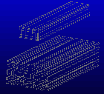
I'm simulating the quality factor of a planar circular coil without ground plane. When I'm simulating I notice that the result is a function of modelling with or without finite thickness. How is this possible ?
1) Any suggestions ?
2) Are their volunteers which would like to run their sim software on my very simple geometry ? This will help to evaluate software
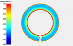
PROBLEM
------
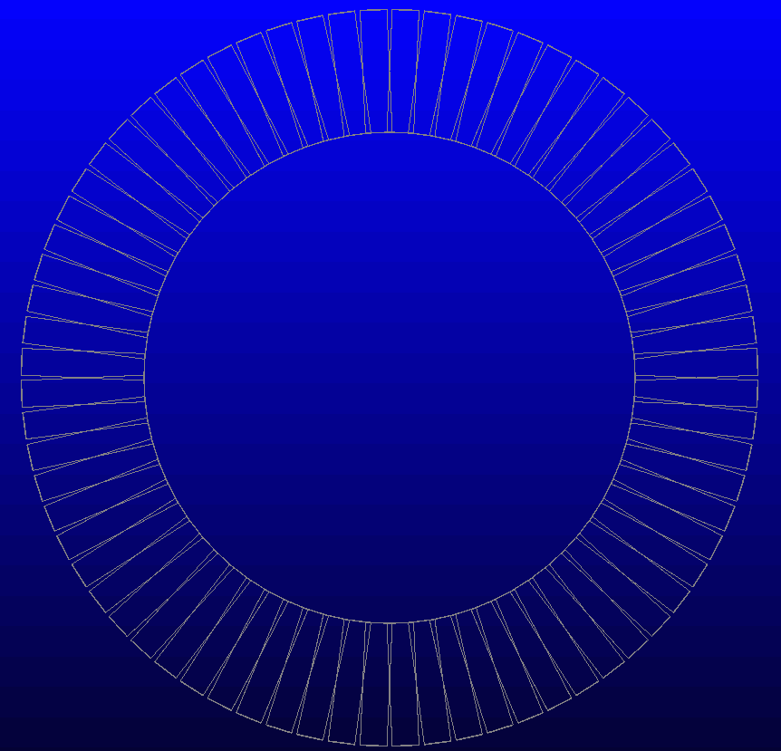
Average diameter : 30 mm
trackwidth: 6mm
thickness = 70 micron
frequency: 50 MHz
-------
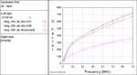
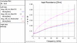
SONNET
--------
Thin Metal: Q = 320 (by volker)
Thick metal Q = 570 (by volker)
Thick metal Q = 380 (by volker, finer meshing)
Thick metal Q = 490 ( by sonnet support on 90 degree section)
--------
AXIEM
-------
Thin metal: Q= 330 (by me)
Thick metal: Q = 500 (by me)
-------
QUICKFIELD
--------------
Q = 440 (by FvM)
FASTHENRY
--------------
Q=500 (by Fvm)
MEASUREMENT
--------
Q = 350 (by me)
possible errors under research: etch angle, contact resistance, solderering, placement capacitor
Please add your simulation result in this topic. Will be VERY appreciated !
Hi,
I'm simulating the quality factor of a planar circular coil without ground plane. When I'm simulating I notice that the result is a function of modelling with or without finite thickness. How is this possible ?
1) Any suggestions ?
2) Are their volunteers which would like to run their sim software on my very simple geometry ? This will help to evaluate software
PROBLEM
------
Average diameter : 30 mm
trackwidth: 6mm
thickness = 70 micron
frequency: 50 MHz
-------
SONNET
--------
Thin Metal: Q = 320 (by volker)
Thick metal Q = 570 (by volker)
Thick metal Q = 380 (by volker, finer meshing)
Thick metal Q = 490 ( by sonnet support on 90 degree section)
--------
AXIEM
-------
Thin metal: Q= 330 (by me)
Thick metal: Q = 500 (by me)
-------
QUICKFIELD
--------------
Q = 440 (by FvM)
FASTHENRY
--------------
Q=500 (by Fvm)
MEASUREMENT
--------
Q = 350 (by me)
possible errors under research: etch angle, contact resistance, solderering, placement capacitor
Please add your simulation result in this topic. Will be VERY appreciated !
Last edited:
")