dsj_guilin
Junior Member level 1
Hi all,
I am new with the layout. I finished a tutorial of layouting an inverter. Now I am doing a layout for a very simple circuit (1*NMOS + 1*cap). I got 2 errors from the DRC (with switch of "no_coverage ") which are:
Figure Causing Multiple Stamped Connections.
Figure Having Multiple Stamped Connections.
Could any one help me to solve them?
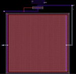
Figures of schematic and layout are attached.
Many thanks.
I am new with the layout. I finished a tutorial of layouting an inverter. Now I am doing a layout for a very simple circuit (1*NMOS + 1*cap). I got 2 errors from the DRC (with switch of "no_coverage ") which are:
Figure Causing Multiple Stamped Connections.
Figure Having Multiple Stamped Connections.
Could any one help me to solve them?
Figures of schematic and layout are attached.
Many thanks.