Continue to Site

Welcome to EDAboard.com

Welcome to our site! EDAboard.com is an international Electronics Discussion Forum focused on EDA software, circuits, schematics, books, theory, papers, asic, pld, 8051, DSP, Network, RF, Analog Design, PCB, Service Manuals... and a whole lot more! To participate you need to register. Registration is free. Click here to register now.

cascode amplifier design

Status
Not open for further replies.

serhannn

Member level 4
Joined
Sep 28, 2010
Messages
69
Helped
2
Reputation
4
Reaction score
2
Trophy points
1,288
Activity points
1,939
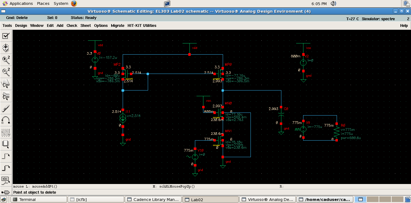
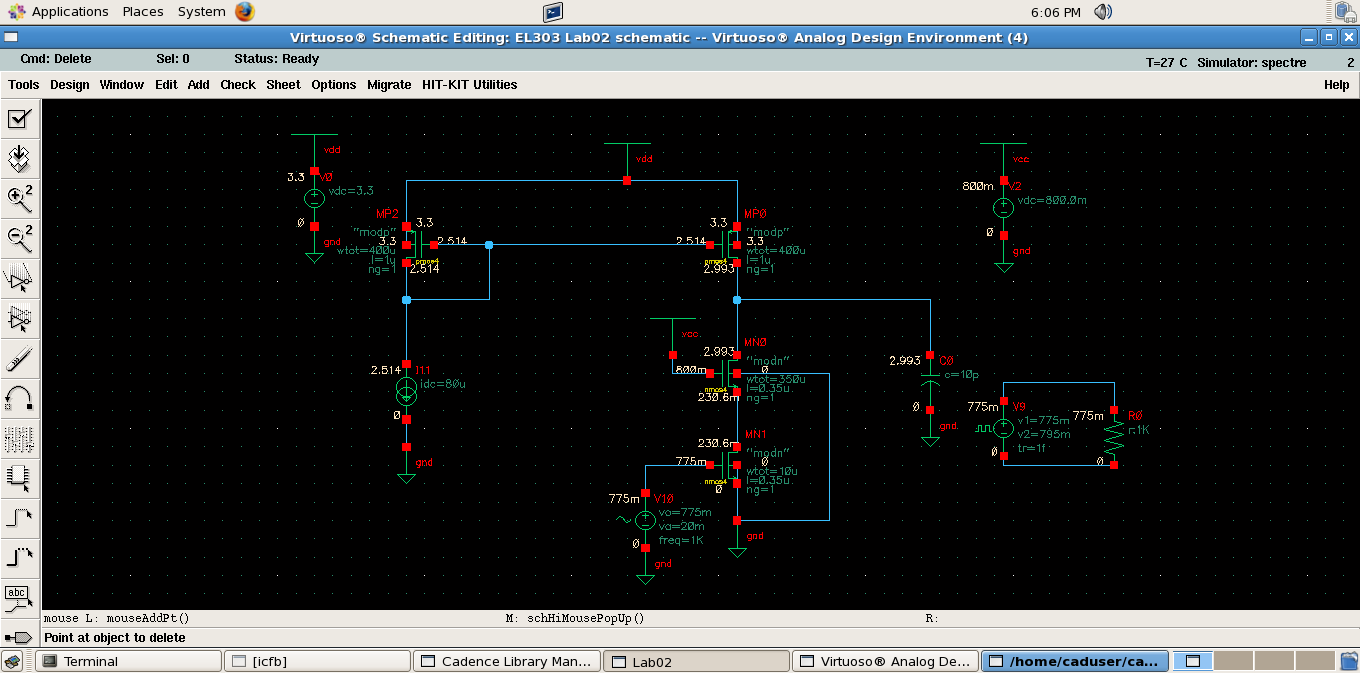
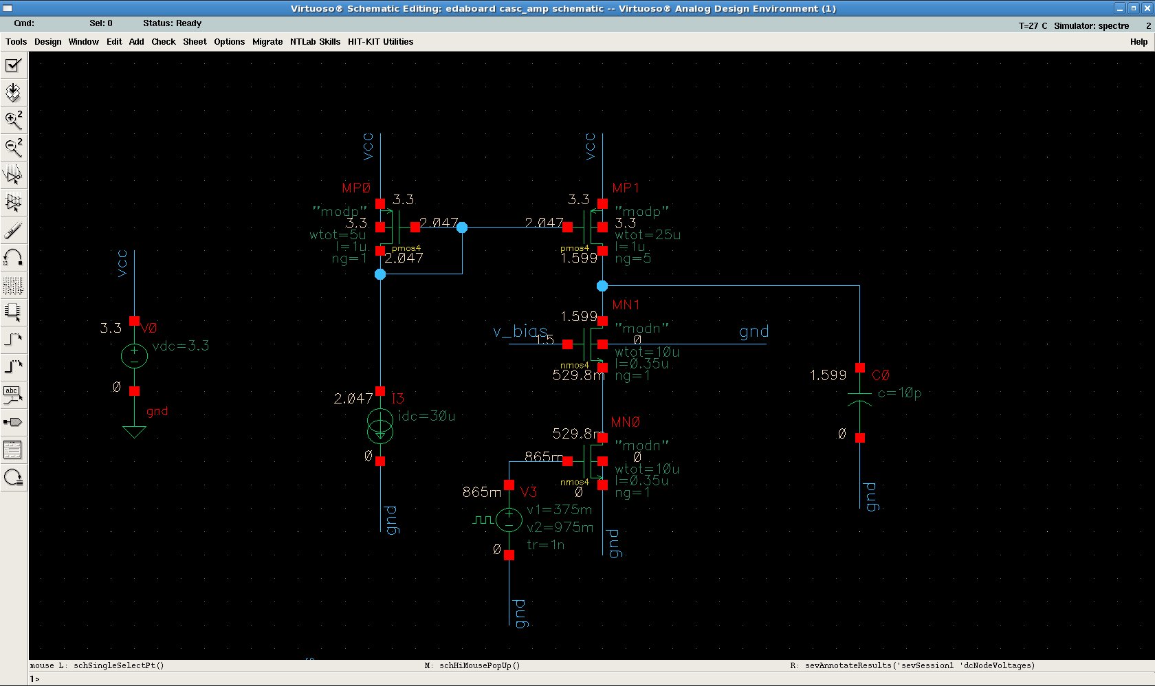
I need to design a cascode amplifier. Specifications are Vdd=3.3V, Power Consumption= 1mW, Gain=50 V/V, Output Swing rate 1.3V (Vmax=2.5, Vmin=1.2) and slew rate with a 10pF load should be 10V/μs or greater. Figure is included.

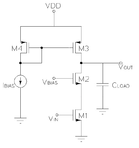
My problem is, I get a much lower slew rate (even lower than 1 V/μs) when I design for a 50 V/V gain and a power consumption less than 1 mW. I know I should increase the bias current to meet that but when I do this, the power consumption obviously increases a lot and also with a higher bias current I can't seem to get the desired gain. What should be the design approach here? I use a bias current of 75μA. Should I start with a much higher one and arrange for the slew rate first and then worry about the gain and swing range? What are your advices?

Thank you.

85_1288170784.jpg
 

Hello
Is this schematic of the whole amplifier - i think some bias circuitry is missing.
And could you pls upload testbench circuits for measuring gain and slew rate.
 

Hi, yes this is the schematic of the whole amplifier. As you see, we are only using a cascode amplifier and a current mirror for the bias current.
I added the circuit schematic with the transistors parameters that I'm using now, also the gain and slew rate measurements. (Gain is measured for a 1 V signal.)


10V/us @ 10pF load => At least 100uA of biasing current!
And don't stinge on current, for 1mW @ 3.3V, you can afford 300uA. Use a N:1 mirror for the high-side, so you can save on the biasing current.
To increase the output impedance for MP0 by increasing L. You have 0.8V headroom on the high side, you dont need such a big W for MP0 to achieve that.
For MN0 and MN1, increase L for a larger output impedance. Adjust W for these transistors just that it is sufficient for the required 1.2V headroom on the low side.
 
Thank you very much for your help and modifications. It has been a great help for me, I couldn't seem to achieve the desired specs whatever I've done.
Can you please also explain how you started your design approach. That would be of great help for my future designs. Also, I have some specific questions. I couldn't figure out what kind of an effect it has to increase the number of gates of MP0 in the circuit. Did you first arrange the bias current or the W/L ratios of the transistors and how did you decide to what to use as bias voltages and current? That would really help a lot for me to understand the basic principles.
Thanks a lot.
 

Hello
let me note some little drawbacks of your initial circuit
- when you need to use transistor with dimensions like 350/0.35 um (i.e. Its width considerably larger than length) always use multiple gates – 10/0.35 um, ng=35. There are several reasons of doing this. Layout dimensions of first transistor would be near 350 um *5 um, of the second – 10 um * 40 um it much more compact. And the second reason is that gate resistance of second one would be considerably smaller than that of the first.
- You have used current mirror with 1:1 ratio – so half of current consumed by your circuit appears unused – that's luxury for low-power applications. So use current mirrors with 1:5 or 1:10 ratio to save current and thus lower power consumption.
- You set the bias for cascode transistor equal to 800 mV – that's too low, because drain voltage of common-source transistor is near 200 mV – that's mean it is biased may be not in triode region, but near of it – so you have lack of gain and speed.
As for my design approach – it's very simple. At first i determined that with SR = 10 V/us and 10 pF load minimum current would be 100 uA. I set it 150 uA for sure. The bias voltage 1.5 V set rather arbitrarily – it should be not less than 900 mV - 1V for common source transistor was biased in saturation. Than i use DC analysis to determine at what dc input voltage level neither current mirror transistor nor cascode would be in triode region. This voltage appears to be near 675 mV.
That's all.
 
  • Like
Reactions: fikea

    fikea

    Points: 2
    Helpful Answer Positive Rating
Status
Not open for further replies.

Similar threads

Part and Inventory Search

Welcome to EDABoard.com

Sponsor

Back
Top