Continue to Site

Welcome to EDAboard.com

Welcome to our site! EDAboard.com is an international Electronics Discussion Forum focused on EDA software, circuits, schematics, books, theory, papers, asic, pld, 8051, DSP, Network, RF, Analog Design, PCB, Service Manuals... and a whole lot more! To participate you need to register. Registration is free. Click here to register now.

100A inverter welder ( IGBTs keep blowing)

Status
Not open for further replies.

salah_edu

Junior Member level 1
Joined
Mar 28, 2008
Messages
17
Helped
0
Reputation
0
Reaction score
0
Trophy points
1,281
Activity points
1,399
Hello,

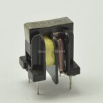
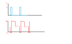
I am trying to design a 100A smps for welding , the design is two switch ( IGBT) forward converter using current transformer for feedback in primary current, the switching tranformer
is a commercialy available toroid transfomer recovred from already working welder , the issue is when i connect the board to ac mains and after a few seconds the ibgts fail without getting hot and they are shorted between ( Gate Emitter and collerctor) i tried to add a capcitor for 22nf beween Gate and emiiter to remove miller effect but i still have the same issue.
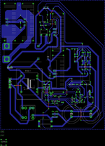
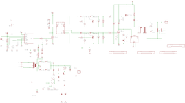
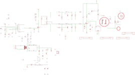
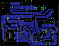
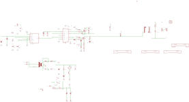
you find attached the schematic and the pcb layout.
Regards.
 

Attachments

  • layout.png
    layout.png
    80.4 KB · Views: 400
  • schematic.png
    schematic.png
    49.8 KB · Views: 471

Hi

The failure description soinds like overvoltage.
Do you have a scope to show the signals?

Klaus
--- Updated ---

Added:

You talk about IGBT
* but I see Mosfets only
* which one gets defective?

Other possible issues:
* bad pcb layout
* missing power supply capacitors
 
Last edited:

    salah_edu

    Points: 2
    Helpful Answer Positive Rating
thank you for the reply.
I use Mosfet only for software footprint , in reality i use the IRG4PC50K Igbts, for C13 and C12 i added themto remove the miller effect but i can remove them,
i connected the scope between collector and emitter of both igbt , but i found that there is a negative voltage of about -50V when the igbts are off, i dont know where it comes from even when i use IGBTs with antiparalelle diode i still have this negative voltage.
 

The PCB layout is not suitable for switching power applications.
It violates many rules ... I recommend to do some PCB layout courses.

I don't know what's the input voltage or output voltage ... but I guess there will be some dangerous high ones...
I see no clear isolation line, thus I guess there is a safety problem, too.
Safety first: Solve the safety problems first.

Klaus
--- Updated ---

I use Mosfet only for software footprint , in reality i use the IRG4PC50K
A good way not only to confuse us, but also yourself.

May I ask:
Do you have any experience in designing switching power circuits?

Klaus
 
Last edited:

The PCB layout is not suitable for switching power applications.
It violates many rules ... I recommend to do some PCB layout courses.

I don't know what's the input voltage or output voltage ... but I guess there will be some dangerous high ones...
I see no clear isolation line, thus I guess there is a safety problem, too.
Safety first: Solve the safety problems first.

Klaus
Ok for the Pcb layout , i will route it again, but do you have an idea where this negative VCE come from even with antiparalelle diodes on the transistors , the supply voltage is +310VDC and output is current limited with R4 potentiometer.
 

i am using this current transformer for sensing 1:300 is it suitable for my application , it is a from china and i could not find any datasheet.
 

Attachments

  • 3pcs-lot-UU10-5-300-1-welding-transformer-filter-for-Inverter-DC-Welding-machine.jpg
    3pcs-lot-UU10-5-300-1-welding-transformer-filter-for-Inverter-DC-Welding-machine.jpg
    42.4 KB · Views: 120

Hi,

obviosly we can not have more information of with this "unknown" current tranformer than you have...
So it´s impossible for us to tell you whether it´s good or not.

In most cases a current transformer is a safety device, because it has to isolate dangerous high voltage from the other circuitry. Thus it needs to fulfill safety standards. (your PCB layout needs to fulfill safety standards, too)
If you (as the designer) - because of lack of datasheet - can not be sure about the safety (or other device specifications), but still use it, then you personally are responsible if any user gets hurt or killed.

--> I´d not use a device without true datasheet. Especially not if it´s a safety device .. but I generally avoid to use even simple devices without datasheet.

Klaus


    salah_edu

    Points: 2
    Helpful Answer Positive Rating
When you work with bypassing not all caps, for the same value, have the same performance
in bypassing effectiveness, eg. ESR.

iu


Regards, Dana.
 

    salah_edu

    Points: 2
    Helpful Answer Positive Rating
If you do not know what bus decoupling it - then you are in for a thin time my friend ...
i mean the HV DC bus or the driver DC Bus !! i dont know the HV +320DC is decoupled with 2,2µF ceramic capacitor but for the gate drive ther is no decoupling
 

No matter if circuit and layout have expectable flaws or you are copying a known working design, you'll start test operation with increasing voltage from a current limited power supply, carefully observing relevant voltage and current waveforms. Making a "big bang" test as you apparently did isn't recommended.

I agree with the critical comments about layout of the primary switching circuit, but I'm also unable to read sense into the output circuit. Where are the output terminals, how about a storage inductor? A two-switch forward converter definitely needs it. How's the rectifier circuit expected to carry 100 A?
Thanks Fvm
is it possible to limit the mains power supply current to 20A or 30A? , for Storage inductor i am using a transformer from an old Inverter Welder, you find attached the transformer and output terminal
--- Updated ---

here are the waveforms with 60w light bulbe in series before the main rectifier
 

Attachments

  • schematic2.png
    schematic2.png
    65.8 KB · Views: 228
  • Sans titre.png
    Sans titre.png
    7.4 KB · Views: 154
Last edited:

why draw the pulses with paint and not attach a picture of your scope ? Anyway that waveform seems weird , are you sure your IGBT doesn't go over rated amperage? When the IGBT fail do your circuit braker trip ?


As other have pointed out, most likely cause is ringing which is induction of high voltage due to strong B fields during switching , if the circuit board is not designed carefully such induction can lead to excessive voltage to accumulate on the traces and destroy mosfets and IGBT and other semiconductors.
Semiconductors are very very fragile with overvoltage and high voltage. One peak and your transistor is DEAD.
You should use an autotransformer that can be regulated and start with no more than 50v AC input, attach a different small transformer for your IC power supply so that the gate driver IC gets enough voltage to work , then you can scope the IGBT and see where and what happens without them failing all the time.
 

    salah_edu

    Points: 2
    Helpful Answer Positive Rating
I have routed the pcb again please take a look if it is good, i have removed the unkown current sense transformer with 0.1ohm sense resistor , i have also removed the gate drive transformer with IR2110 gate driver ic, is this layout best then the first one ?
 

Attachments

  • pcb3.png
    pcb3.png
    50.5 KB · Views: 167
  • schematic3.png
    schematic3.png
    41.2 KB · Views: 200

Maybe just maybe it is the sense circuitry that is causing problems.
The overall schematics looks fine to me. I can say from experience that designing feedback is often the most complicated part. I once made a SMPS and had to take out the optocoupler feedback regulation because that destabilized the driving for the switches.
The reason this can happen is because the feedback attempts to change the either frequency or pulse width of the transistors under varying load and if not done properly it can cause certain bad outcomes like both transistors conducting at the same time etc.
Thanks Salvador12,

i have tested the circuit yesterday and it is working without blowing igbts only i have another problem know, with the 0.1ohm sense resistor i hope to get 10A in the primiray because of 1V voltage sense on the UC3845 pin 3 , but when i short circuit the secondry i could not get 30Amps in the secodery i wish to have because my power transformer have 28winding in the primary and 4 winding in the secondry part 28:4 , my be i need to lower again the sense resistor ??
 

Status
Not open for further replies.

Similar threads

Part and Inventory Search

Welcome to EDABoard.com

Sponsor

Back
Top