Continue to Site

Welcome to EDAboard.com

Welcome to our site! EDAboard.com is an international Electronics Discussion Forum focused on EDA software, circuits, schematics, books, theory, papers, asic, pld, 8051, DSP, Network, RF, Analog Design, PCB, Service Manuals... and a whole lot more! To participate you need to register. Registration is free. Click here to register now.

100A stick welder standby current

Status
Not open for further replies.

salah_edu

Junior Member level 1
Joined
Mar 28, 2008
Messages
17
Helped
0
Reputation
0
Reaction score
0
Trophy points
1,281
Activity points
1,399
Hi All;

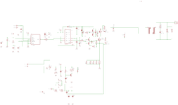
i have designed a 100 A stick welder using two switch forward converter topology , i used a switching transformer from an old igbt inverter welder , my problem is that the standby current is too high and the igbts are too hot, i tried to increase the switching frequency from 70khz to 140khz but the idle current is still too high, i tried also to reduce the gate resistor to reduce the switching loss but there is no improvement in igbts temperature , the current sensing resistor are five 100 mohm in paralelle connected to the low side switch in primary current.
you find below the schematic and the pcb.
can you please help me to investigate this problem?
another question does a transformer need a target frequency to reduce the primary idle current?
 

Attachments

  • arcwelder.png
    arcwelder.png
    40.7 KB · Views: 96
  • arcwelderpcb.png
    arcwelderpcb.png
    79.4 KB · Views: 98

Why are you using a driver IC with 2A output capability to drive two small transistors then the MOSFETs. The IC is designed to drive MOSFETS directly and you will get better and faster switching if you do so.

The voltage drop in D5 also means you have less supply to the top MOSFET.

You also seem to be driving almost the same waveform to both sides of the transformer.

D8 also seems to be directly across VCC with no current limiting - not a good strategy when it is only rated at 500mW.

Brian.
thank you brian,
i used the two transistors because the igbt are far from the control ic and to reduce the noise due to long traces and high frequency.
about the d5 voltage drope , i think it is not so important because the drive supply voltage is 18v and even with 0.7v forward voltage it can turn on the IGBT well.
for d8 i think you are right.
 

Him

the schematic (drawing skills) could be improved. It´s hard do read because of
* open ends
* useless edges
* missing junction dots
* missing part values.

Also the schematic (circuit design) is rather confusing.
* What are the BC327 for? I see no benefit, making everything worse. They reduce current, reduce voltage, increase delay ...
* the complement information to BC327 is completely missing
* I can´t find IRFPC40 datasheet
* and so on.

PCB layout misses a clear GND plane and misses short, low stray inductance routing.
Unnecessary bends, unnecessarily changing layers ...

All this probably leads to
* cross conduction
* a lot of ringing

***
My recommendation: Don´t rely on hobbyists circuits. Read through some application notes on high power switch mode circuit design. Read design notes, look for reliable example circuits. Learn how to design properly.

Then desgin the schematic a new. Show it so we can give advice
Then do the PCB design a new. Show it so we can give advice

Klaus
thank you Klaus,

can you please give me a document to learn design correct layout ?
 

hi all,
i have 2kw two switch forward converter using two igbts and toroid transformer,
can you please tell me if this layout is good for such application and does it need more optimisation.
kind regards

schema2.png


routing2.png
 

Hi,

I guess it´s not improved much.
All of post#4 still applies.

can you please give me a document to learn design correct layout ?
I guess every PCB layout software comes with tutorials.
And numerous documents can be found in the internet.
Numerous youtube videos.

Klaus
 

Do you have a scope so that you can examine your gate drive at the IGBT,
to look at supply rails, and to detect if you have RF oscillation in the circuit.

Some ref docs that may help :


Bypass capacitors, for same C, not all equal in performance, eg. esr -

1666104374429.png


OSCON in the chart is tantalum polymer.


Regards, Dana.
 

Not convinced those bipolar boosters betwen the half-bridge
driver and the FETs are a good idea. If the HO output pulls any
DC current (which those BJT bases will) the bootstrap capacitor
might get bled to where high side gate drive is compromised.
You may get more peak drive, but those boosters pull from the
same bootstrap cap so there's no "win" on that account, only
(perhaps) edge rate on the gate. Yet you are also degrading
that, I guess on purpose, with the series R. So....

Also those BJTs "could" have a transient saturation behavior
(gonna smack a capacitor, at high peak current, and get to
Vce(sat) < Vbe for an interval allowing saturation, and possibly
extending the MOSFET turnoff by saturation recovery time,
then messing with your designed anti-shoot-through. But at
low frequencies this should be a modest switching loss adder.
Was a problem for me in designing bipolar power MOSFET
drivers, when I moved from an all-NPN totam pole to something
similar to yours (emitter follower final) I could see the VOL go
all the way to VEE, then come back up to my Baker clamped
resting voltage, because transient saturation happens faster
than a Baker clamp can prevent. So this imposed a minimum
pulse width low, not a problem for the application at its 10KHz
range chop and near 50% duty, but would have made the
product unsuited to very narrow or wide duty ratios at higher
frequency.

This suggests that you might take a closer look at relation of
standby current to chop frequency, see whether you can pin
the problem on switching or conduction (or, conduction losses
that are taken at switching rate...) to home in on the problem(s).
Might look at the waveforms along the gate-drive lineup and see
if any other aspect of that bipolar-buffer scheme is costing you
drive-to-min-Idd levels or corrupting the anti-shoot-through
timing you think you're getting.
 

Status
Not open for further replies.

Similar threads

Part and Inventory Search

Welcome to EDABoard.com

Sponsor

Back
Top