Continue to Site

Welcome to EDAboard.com

Welcome to our site! EDAboard.com is an international Electronics Discussion Forum focused on EDA software, circuits, schematics, books, theory, papers, asic, pld, 8051, DSP, Network, RF, Analog Design, PCB, Service Manuals... and a whole lot more! To participate you need to register. Registration is free. Click here to register now.

why a donut transistor has least amount of drain capacitance.

Status
Not open for further replies.

sys_eng

Full Member level 4
Joined
Aug 3, 2016
Messages
193
Helped
0
Reputation
2
Reaction score
1
Trophy points
18
Activity points
1,489
In the book it says
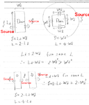
Because the drain area of the donut transistor is shared by the gates in all four sides, the parasitic drain capacitance is
reduced to minimum,

why drain area surrounded by gate has minimum drain capacitance?

Cgd capacitance between gate and drain , if the drain surrounded by gate that means more drain-gate overlap therefore increase the capacitance instead of minimizes it. It doesn't make sense.
donut.jpg
 

Cdb.
For same effective gate width, Cgd is almost same, however Cdb is minimized compared to conventional structure.


But Cdb is from vertical parasitic capacitance meaning drain and its underneath subtrate forms capacitance. it shouldn't have anything to do with a lateral gate surrounding the drain.
 

But Cdb is from vertical parasitic capacitance meaning drain and its underneath subtrate forms capacitance. it shouldn't have anything to do with a lateral gate surrounding the drain.
Simply you are misunderstanding.
Cgd is not minimized.

Minimizing Cdb is important.
 
Last edited:

Simply you are misunderstanding.
Cgd is not minimized.

Minimizing Cdb is important.

OK, no problem with minimize Cdb but how the donut shape can help?
The drain area with P/N junction still exists with the substrate underneath.


as I know, to reduce the Cdb, one can make the drain area smaller.
 

When I used a donut device I estimated the Leff to be the centerline of the gate. That means Cgd will be lower vs a conventional device. Cgs will be higher. The drain area is smaller with no perimeter so no fringe capacitance. Only concern at the time was the single contact on the drain but everything ended up working fine in silicon.
 

When I used a donut device I estimated the Leff to be the centerline of the gate. That means Cgd will be lower vs a conventional device. Cgs will be higher. The drain area is smaller with no perimeter so no fringe capacitance. Only concern at the time was the single contact on the drain but everything ended up working fine in silicon.

Want to reduce Cgd , why not just use finger approach, break the a transistor into smaller pieces, and therefore reduce the drain area?
 

and therefore reduce the drain area?
Cgd can never be reduced even if drain area is smaller.
Cgd is determined by effective gate width.
And an electrode for drain is required which overwrap gate.
So Cgd of donut MOS is slightly larger compared to conventional structure.

On the other hand, Cdb can be reduced.
 

Cgd can never be reduced even if drain area is smaller.
Cgd is determined by effective gate width.
And an electrode for drain is required which overwrap gate.
So Cgd of donut MOS is slightly larger compared to conventional structure.

On the other hand, Cdb can be reduced.

OK, I now agree Cgd cannot be reduced by smaller drain area.
look at the diagram, Cdb is vertical, it's going down.
how did the donut shape help?

cap.jpg
 

It's not the drain C, but the ratio of Cdg and Cdb (the
former mattering much more to everything but RF
linearity) to drive current and gm. The "donut" uses
all of the drain periphery. A minimum 2-finger FET uses
only half. A minimum 1-finger FET uses 1/4.

You pay for it in Cgs, which may or may not be a
desirable trade. You also lose symmetry and likely see
worse hot carrier degradation and oxide wearout. But
sometimes there are better reasons for, than against,
in sum.


well, others are saying Cgd is the most affected feature while you keep on saying Cdb,

you didn't explain the donut feature reduce drain capacitance with relationship to Cdb.

- - - Updated - - -

It's not the drain C, but the ratio of Cdg and Cdb (the
former mattering much more to everything but RF
linearity) to drive current and gm. The "donut" uses
all of the drain periphery. A minimum 2-finger FET uses
only half. A minimum 1-finger FET uses 1/4.

You pay for it in Cgs, which may or may not be a
desirable trade. You also lose symmetry and likely see
worse hot carrier degradation and oxide wearout. But
sometimes there are better reasons for, than against,
in sum.


OK, donut use all 4 sides of drain, That means the gate to drain overlap should increase 4x therefore Ggd should be 4x.
 

others are saying Cgd is the most affected feature while you keep on saying Cdb
We can reduce Cgd by cascode topology.

However we can never reduce Cdb by any circuit topology.

OK, donut use all 4 sides of drain,
That means the gate to drain overlap should increase 4x therefore Ggd should be 4x.

You can not understand anything at all.

Cgd is determined by effective gate width.

On the othehand, Cdb is determined by drain area.

Drain area of Donut MOS is minimum compared to conventional structure which have same effective gate width.

Surely consider before posting.
 

Drain area of Donut MOS is minimum compared to conventional structure which have same effective gate width.

why?

We are running in circle. You been saying the statement for many times already and I have asked many times why.
 

Cgdo is larger. But effective width is set at the source which
is -much- larger. As an example annular devices I have laid out
have 0.42u square drains and 2.16um Weff at the minumum size
for a 5V NMOS, while the minimum straight gate is 0.42/0.6um.
So Cgdo "width" is 4X (1X of which you'd eat no matter what)
but Weff is >5X. And Cdb0 is 0.42^2 instead of 0.42*2.16. Not
a huge win, but better ratio-wise.

But this is all a waste of time discussing, for a couple of reasons.
Leaving aside intellectual laziness, nobody really uses these
annular devices because of some capacitance benefit. There
are indeed reasons, but this has never been one. Maybe the
real answer is that off-the-cuff remarks in some professor's
class notes off the Internet just aren't relevant to anything.

And thus so too, the endless "Why? Why? Why?" about it.
 

Status
Not open for further replies.

Part and Inventory Search

Welcome to EDABoard.com

Sponsor

Back
Top