Continue to Site

Welcome to EDAboard.com

Welcome to our site! EDAboard.com is an international Electronics Discussion Forum focused on EDA software, circuits, schematics, books, theory, papers, asic, pld, 8051, DSP, Network, RF, Analog Design, PCB, Service Manuals... and a whole lot more! To participate you need to register. Registration is free. Click here to register now.

A question about class C amplifier design?

Status
Not open for further replies.

samy555

Full Member level 4
Joined
May 11, 2010
Messages
207
Helped
0
Reputation
0
Reaction score
0
Trophy points
1,296
Location
Palestine
Activity points
2,963
Hi
I have read many of the pages on the Web about class C amplifier, and I have benefited and learned a lot, but unfortunately non of these sites spoke about how to choose the values of C1 and R1 (look at the circuit below).

111.jpg

I think that C1 & R1 form a HPF, if the input signal is of 2V peak and 10MHz frequency, I think that if you choose to value of C1 such that it has very low reactance at 10MHz then using the high pass RC filter law to calculate R1 when cutoff freq = 10MHz or lower.
Thanks
 
Last edited by a moderator:

Re: A qUestion about class C amplifier design?

With a high impedance at resonance, Class C offers high gain and high Q , convert pulse to sine, high efficiency but poor impedance gain (buffering), noise filtering. Add a small emitter R for better linearity and avoid Vce<2V.

Of course choose R to control current for maximum hFE gain or current drain and Choose C to reject unwanted noise.

Consider source impedance must be fairly low if Re=0 but depends on current(rBE) and hFE. Your simulation Zsource=0

Then consider what do you want to gain?
power? voltage ? Current? impedance? SNR? or some of the above?

Then define your specs for Zin/out & Vin/out and decide which config is best.
 

Re: A qestion about class C amplifier design?

I think that C1 & R1 form a HPF

R1 and C1 are not working as a HPF, they are responsible to produce narrow pulses of base current. As a result, the transistor conducts for only a fraction of the RF cycle.
 

Providing the time constant of C1 and R1 is long compared to the period of the RF drive, C1 accumalates charge which biases the transistor off. So if you increase the drive level the transistor conducts for a shorter time and the current pulses get narrower.
Frank
 

Thank you very much SunnySkyguy and ahsan_i_h

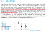
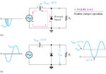
I read in a book (Electronic Devices and Circuit Theory 7th Edition) page 83:
111.jpg
112.jpg
113.jpg

Now, if the operating frequency of my class C amp. = 10MHz, then T = 1/f = 0.1 usec and 0.5T = 0.05 usec
5RC (= 5 * time constants) should be much greater than 0.05 usec that is 5*RC = at least 10 * 0.05 usec
RC >= (10 * 0.05 usec)/5 = 0.1 usec
In general: RC >= 10*(1/2f)/5
RC>= 1/f
Design Steps:
Choose C1 so that Xc1=0.1 ohm at the operating freq

114.jpg
C1=160 nF
R1 >= 1/(C1 * f)
R1 >= 0.625 ohm nooooooooooooooooooooo,,, there is something wrong
Help me please
 

My Design Steps;
Choose ZL >> Zs for low attenuation
  1. Determine Source impedance,Zs and desired Load Impedance, ZL.
  2. Choose C such that Zc(f) <1% of ZL for low attenuation
    where Zc=1/(2pi*f*C)
  3. Choose diode such that Vf of diode<< Vin for low offset ( i.e. Schottky or Silicon)
  4. Choose diode power rating such that 1/Pd~ESR is << ZL e.g. 100mW diode ~ 10Ω, 1W Diode~1Ω , for high Z, don't neglect diode capacitance

e.g.
Assume Zs=10k, let ZL>=100k, assume Vin = 5V ,
Let Zdiode<<1k so any small signal Schottky diode or pin diode for microwave.
if Zc<=1% of ZL @10MHz or 1% of 100k, then Zc <1kΩ
since Zc=1/(2pi*f*C)
thus C>=1/(2pi*f*1kΩ) = 1/6.28*1e9 = 0.16 nF


[*]Choose diode such that Vf of diode<< Vin for low offset ( i.e. Schottky or Silicon)
[*]Choose diode power rating such that 1/Pd~ESR is << ZL e.g. 100mW diode ~ 10Ω, 1W Diode~1Ω , for high Z, don't neglect diode capacitance
[*]
[/LIST][/SIZE]

It seems to me you did not read the subject from the beginning. Diode here represents the B-E junction of the transistor.

e.g.
Assume Zs=10k, let ZL>=100k, assume Vin = 5V ,
Let Zdiode<<1k so any small signal Schottky diode or pin diode for microwave.
if Zc<=1% of ZL @10MHz or 1% of 100k, then Zc <1kΩ
since Zc=1/(2pi*f*C)
thus C>=1/(2pi*f*1kΩ) = 1/6.28*1e9 = 0.16 nF
Once again it seems to me I will use a microstrip capacitor (0.16 nF !!!!!)

Thank you
 

samy555, I believe you missed an important aspect of this class C amplifier circuit.

Although R1 can be seen as a part of a high pass filter, it's also sourcing the transistor base current. So the resistance value must not be too high, otherwise you are loosing available output power.

A complete circuit specification that includes generator impedance, transistor parameters, tank circuit and output load will allow you to evaluate the effect of R1/C1 dimensioning in a simulation.
 

It seems to me you did not read the subject from the beginning. Diode here represents the B-E junction of the transistor.


Once again it seems to me I will use a microstrip capacitor (0.16 nF !!!!!)

Thank you
It seems I may not understand your objective.

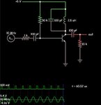
Here is a 100mV pulse driven resonant circuit.

Notice the base is biased all the time giving continuous current and lower distortion with >2x Vcc output into a 10K load. ( based on a loaded Q.)

The input cap is just for AC coupling not diode clamping.

class C.jpg

The difference in peak voltages of Sine out is an indication of asymmetry. from Vce saturation.

An improvement on this would have negative feedback on peak amplitude to prevent saturation or a higher impedance load.
 

It seems I may not understand your objective.

Here is a 100mV pulse driven resonant circuit.

Notice the base is biased all the time giving continuous current and lower distortion with >2x Vcc output into a 10K load. ( based on a loaded Q.)

The input cap is just for AC coupling not diode clamping.

View attachment 120776

The difference in peak voltages of Sine out is an indication of asymmetry. from Vce saturation.

An improvement on this would have negative feedback on peak amplitude to prevent saturation or a higher impedance load.
First your transistor operates in class A mode not in class C.
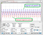
Second: in the following class C amp:
11.jpg

The input signal applied at point A is a 5Vp sinewave of 10MHz freq. Please look how the sig is clamped due to the B-E junction diode:
12.jpg

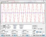
And finally, the output signal (after changing the input signal freq to 5.19MHz to tune with the tank circuit):
13.jpg

My question was: On what basis C1 and R1 are calculated?
Thank you.

- - - Updated - - -

I read in a book (Electronic Devices and Circuit Theory By Floyd,9ed) page 69:
11.jpg
12.jpg
13.jpg

Based on these excellent information, I'll repeat design on the grounds that Xc1 = 1 ohm at the oprating freq, then I will calculate resistance so that RC = 100/freq, any comment?
 

Status
Not open for further replies.

Similar threads

Part and Inventory Search

Welcome to EDABoard.com

Sponsor

Back
Top