designer_ec
Member level 4
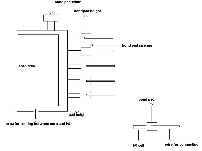
die area, core area
Please anybody tell me that in P&R when we are doing floor plan how to decide Die size for chip level and how to decide core size.Please inform me if there is any formlas to calculate those sizes or if any thumb rule for that calculation.
Please anybody tell me that in P&R when we are doing floor plan how to decide Die size for chip level and how to decide core size.Please inform me if there is any formlas to calculate those sizes or if any thumb rule for that calculation.